Semiconductor device and manufacturing method for same

a technology of semiconductors and manufacturing methods, applied in semiconductor devices, basic electric elements, electrical equipment, etc., can solve the problems of difficult formation of a region, scratching of implanted faces, thin wafer breakage, etc., and achieves a wide buffer structure, low loss, and fast operation

Active Publication Date: 2008-12-25
FUJI ELECTRIC CO LTD
View PDF1 Cites 82 Cited by
  • Summary
  • Abstract
  • Description
  • Claims
  • Application Information

AI Technical Summary

Benefits of technology

[0024]In order to resolve the above-described problems of the prior art, the invention provides a broad buffer structure diode, IGBT, or other power semiconductor device, with fast operation and low losses, and which has soft switching characteristics. The invention also provides a manufacturing method for a semiconductor device, which is a broad buffer structure diode, IGBT, or other power semiconductor device, with fast operation and low losses, and which has soft switching characteristics, inexpensively, with good controllability and good yields, using FZ bulk wafers.
[0032]By means of a semiconductor device of the present invention, a diode, IGBT, or similar with a broad buffer structure, with fast operation and low losses, and having soft switching characteristics, is obtained. Further, by means of a semiconductor device manufacturing method of the present invention, diode, IGBT, or similar with a broad buffer structure, with fast operation and low losses, and having soft switching characteristics, can be manufactured inexpensively, with good controllability and good yields, using FZ bulk wafers.

Problems solved by technology

It is difficult to form a region with a higher donor concentration than the initial phosphorus concentration of a semiconductor substrate deep in the bulk material through ion implantation of phosphorus and arsenic as normal donor atoms.
Hence there are the problems that the thin wafer may break during handling, the ion-implanted face may be scratched due to foreign matter, or for other reasons a diffusion region with the desired concentration may not be formed.
However, because control of donor concentrations is difficult, there is a problem in that the desired concentration profile cannot easily be obtained.
Hence it is unclear whether a broad buffer structure can actually be fabricated.
Moreover, upon comparing FIG. 3 in Patent Document 5 and FIG. 4 in the same reference, it is seen that compared with the device fabricated by helium irradiation with the desired profile of FIG. 4, the concentration in the high-concentration region of a device fabricated by proton irradiation in FIG. 3 is approximately four times the desired concentration, so that precise control is not achieved.
This is because numerous defects exist in the vicinity of the proton range, and consequently the resistivity is high in the region at this depth.
In this way, using a well-known proton irradiation and heat treatment method, it is difficult to form the desired broad buffer structure.

Method used


Image

  • Semiconductor device and manufacturing method for same
  • Semiconductor device and manufacturing method for same
  • Semiconductor device and manufacturing method for same

Examples


embodiment 1

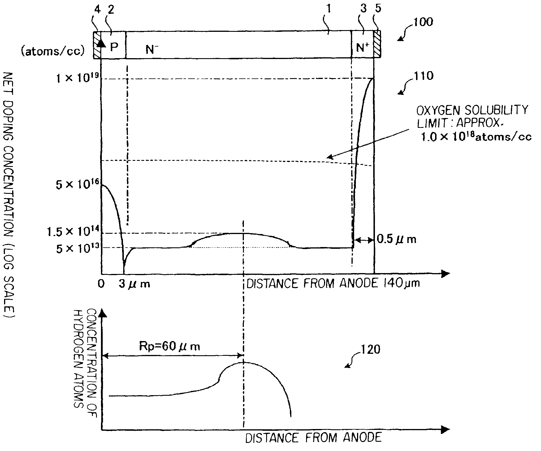
[0087]FIG. 1 shows the configuration of the semiconductor device of Embodiment 1 of the invention, the net doping concentration, and the distribution of hydrogen atoms. In FIG. 1, a P-type second semiconductor layer 2, serving as a P anode layer, is formed on one main face of an N-type first semiconductor layer 1, serving as an N− drift layer, as shown in cross-sectional view 100 of the semiconductor device. Further, an N-type third semiconductor layer 3, serving as an N+ cathode layer, is formed on the other main face of the first semiconductor layer 1. And, on the surface of the second semiconductor layer 2, an anode 4 is formed. And on the surface of the third semiconductor layer 3, a cathode 5 is formed.

[0088]As shown in the characteristic diagram 110 for the distance from the anode and the net doping concentration (log scale) in FIG. 1, the net doping concentration in the first semiconductor layer 1 has a peak substantially in the center of the first semiconductor layer 1, and ...

embodiment 2

[0122]FIG. 12 shows the configuration of the semiconductor device of Embodiment 2 of the invention, the net doping concentration, and the proton distribution. As shown in cross-sectional view 1200 of the semiconductor device in FIG. 12, the semiconductor device of Embodiment 2 is the semiconductor device of Embodiment 1 shown in FIG. 1, with a fourth semiconductor layer 7, serving as an N cathode buffer layer, with higher concentration than the first semiconductor layer 1 and lower concentration than the third semiconductor layer 3, provided between the first semiconductor layer 1 and the third semiconductor layer 3. Otherwise the configuration is the same as in Embodiment 1, and so the same symbols are assigned, and explanations are omitted.

[0123]As an example, the net doping concentrations and dimensions of various portions of a semiconductor device of Embodiment 2 are described. However, only values different from those of the example of Embodiment 1 are explained. As shown in th...

embodiment 3

[0134]FIG. 15 shows the configuration of the semiconductor device of Embodiment 3 of the invention, the net doping concentration, and the distribution of hydrogen concentration. As shown in cross-sectional view 1500 of the semiconductor device in FIG. 15, the semiconductor device of Embodiment 3 is the semiconductor device of Embodiment 1 shown in FIG. 1, in which the third semiconductor layer 3 is made thick. Otherwise the configuration is similar to that of Embodiment 1, and so the same symbols are assigned and explanations are omitted.

[0135]As an example, the net doping concentrations and dimensions of each of the portions of the semiconductor device of Embodiment 3 are described. However, only values different from those of the example of Embodiment 1 are explained. As indicated in the characteristic diagram 1510 for the distance from the anode and the net doping concentration (log scale) in FIG. 15, the distance to the interface between the first semiconductor layer 1 and the t...


PUM


Abstract

After introducing oxygen into an N− type FZ wafer serving as an N− type first semiconductor layer, a P type second semiconductor layer and an anode are formed on a surface of the FZ wafer. The FZ wafer is irradiated with protons from the side of the anode, introducing crystal defects into the FZ wafer. By performing heat treatment to recover the crystal defects in the FZ wafer, the net doping concentration of a portion within the first semiconductor layer is made higher than the initial net doping concentration of the FZ wafer, and a desired broad buffer structure is formed. Accordingly, a semiconductor device with fast operation and low losses, and having soft switching characteristics, can be manufactured inexpensively using FZ bulk wafers, with good controllability and yields.

Description

CROSS REFERENCE TO RELATED APPLICATION[0001]This application is a by-pass continuation application of, and claims priority from, PCT / JP2006 / 322547 filed Nov. 13, 2006, the content of which is incorporated herein by reference, which in turn claims priority from JP2005-329480 filed Nov. 14, 2005.BACKGROUND[0002]The invention relates to a diode or IGBT (insulated-gate bipolar transistor) or other semiconductor device, which has soft recovery characteristics in addition to high speed and low losses, and to a manufacturing method for such a device.[0003]Semiconductor devices for use in power applications include diodes, IGBTs and similar devices in 600 V, 1200 V, 1700 V, and similar classes. Recently, there have been improvements in the characteristics of these devices. Power semiconductor devices are used in high-efficiency, power-conserving converter / inverters and other power conversion devices, and are indispensable for control of rotary motors and servomotors.[0004]Such power control...

Claims


Application Information

Patent Timeline
Patent Type & Authority Applications(United States)
IPC IPC(8): H01L21/322H01L29/36
CPCH01L21/2255H01L21/263H01L29/32H01L29/8611H01L29/7397H01L29/861H01L29/36
Inventor NEMOTO, MICHIO
Owner FUJI ELECTRIC CO LTD
Why Eureka
Try Eureka