Method of manufacturing semiconductor device

a manufacturing method and semiconductor technology, applied in the direction of semiconductor devices, electrical devices, transistors, etc., can solve the problems of inability to provide high-speed operations, increase the resistance of gate and source/drain, etc., to improve the reliability of the semiconductor device and improve the performance of the semiconductor devi

Active Publication Date: 2009-01-08
RENESAS ELECTRONICS CORP
View PDF36 Cites 46 Cited by
  • Summary
  • Abstract
  • Description
  • Claims
  • Application Information

AI Technical Summary

Benefits of technology

[0009]It is preferable that the metal silicide layer to be formed by the salicide process on the surface of the conductive film forming a gate and the semiconductor region forming a source / drain is made of nickel silicide rather than cobalt silicide according to requirements of low resistance due to scaling. By making the metal silicide layer of nickel silicide instead of cobalt silicide, it is possible to make the resistance of the metal silicide layer lower, and to decrease the diffusion resistance, the contact resistance and the like of the source / drain. Further, by making the metal silicide layer of nickel silicide instead of cobalt silicide, it is possible to form the metal silicide layer thinner, and to make the junction depth of the source / drain shallower, thereby obtaining advantages for scaling field effect transistors.
[0024]Further, it is possible to improve reliability of a semiconductor device having a field effect transistor on which a metal silicide layer is formed on a surface of a source / drain.

Problems solved by technology

However, a problem rises that the resistances of the gate and source / drain are increased, and high-speed operations cannot be provided even if the field effect transistor is miniaturized.

Method used


Image

  • Method of manufacturing semiconductor device
  • Method of manufacturing semiconductor device
  • Method of manufacturing semiconductor device

Examples


first embodiment

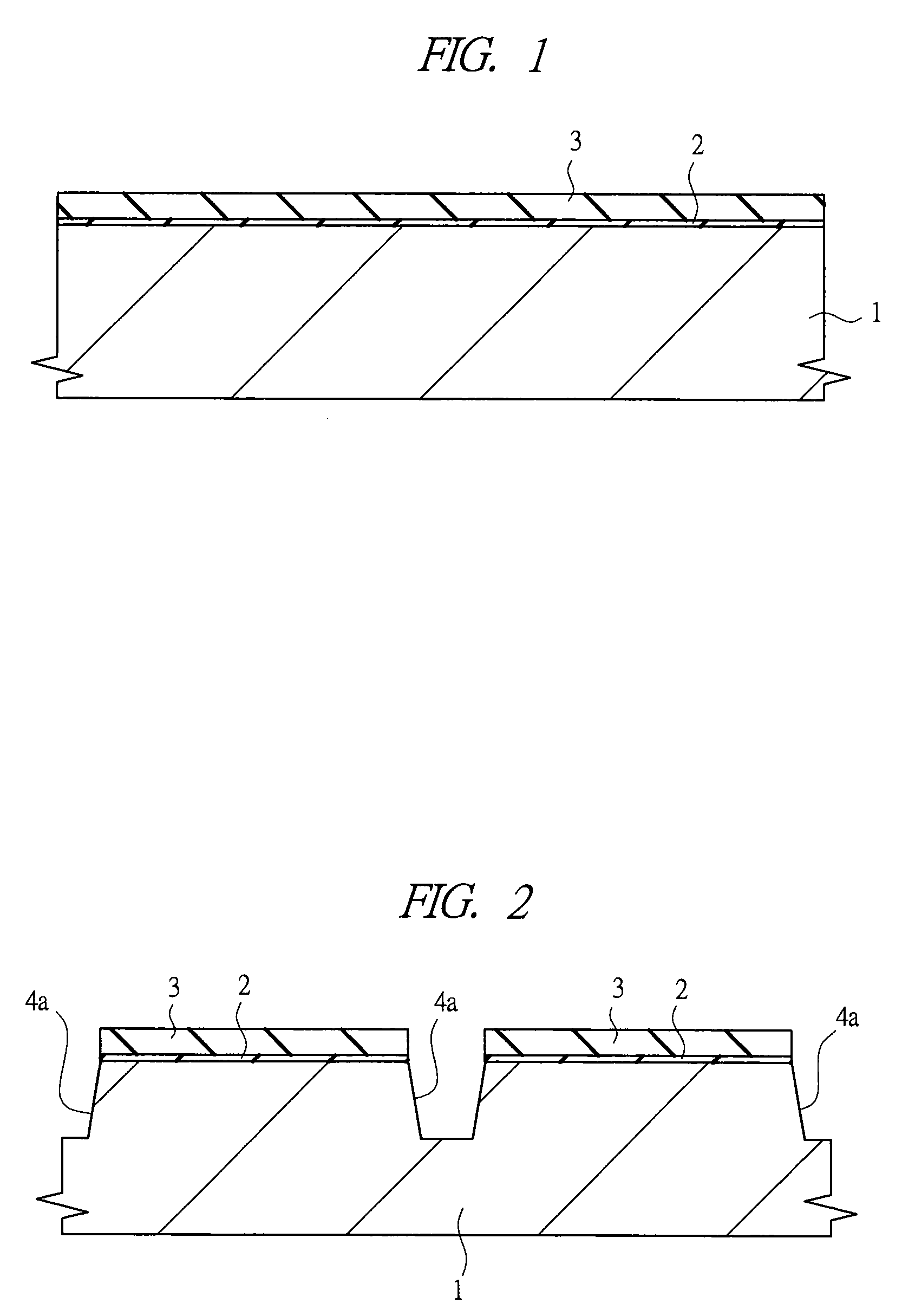
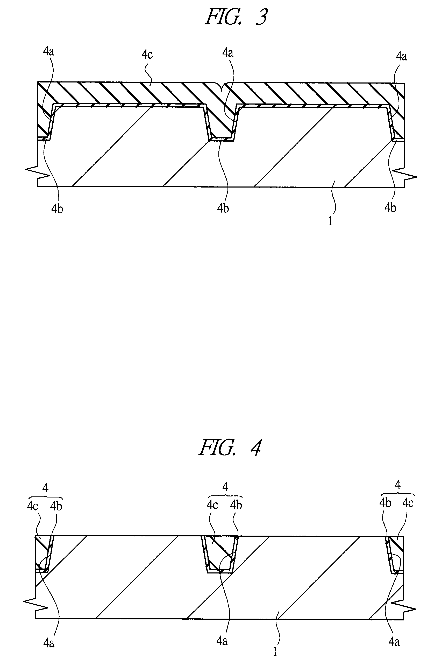
[0092]Manufacturing steps of a semiconductor device according to a present embodiment will be described with reference to the drawings. FIG. 1 to FIG. 8 are cross-sectional views of main parts showing the manufacturing steps of the semiconductor device according to an embodiment of the present invention, for example, a semiconductor device having a CMISFET (Complementary Metal Insulator Semiconductor Field Effect Transistor).

[0093]First, as shown in FIG. 1, a semiconductor substrate (semiconductor wafer) 1 made of p-type single crystal silicon and the like having a resistivity of, for example, about 1 to 10 cm is provided. Next, the semiconductor substrate 1 is subjected to heat oxidation and an insulating film 2 having a thickness of, for example, about 11 nm is formed on the surface of the semiconductor substrate 1, and on an upper layer thereof, an insulating film 3 having a thickness of, for example, about 90 nm is deposited by a CVD (Chemical Vapor Deposition) method and the li...

second embodiment

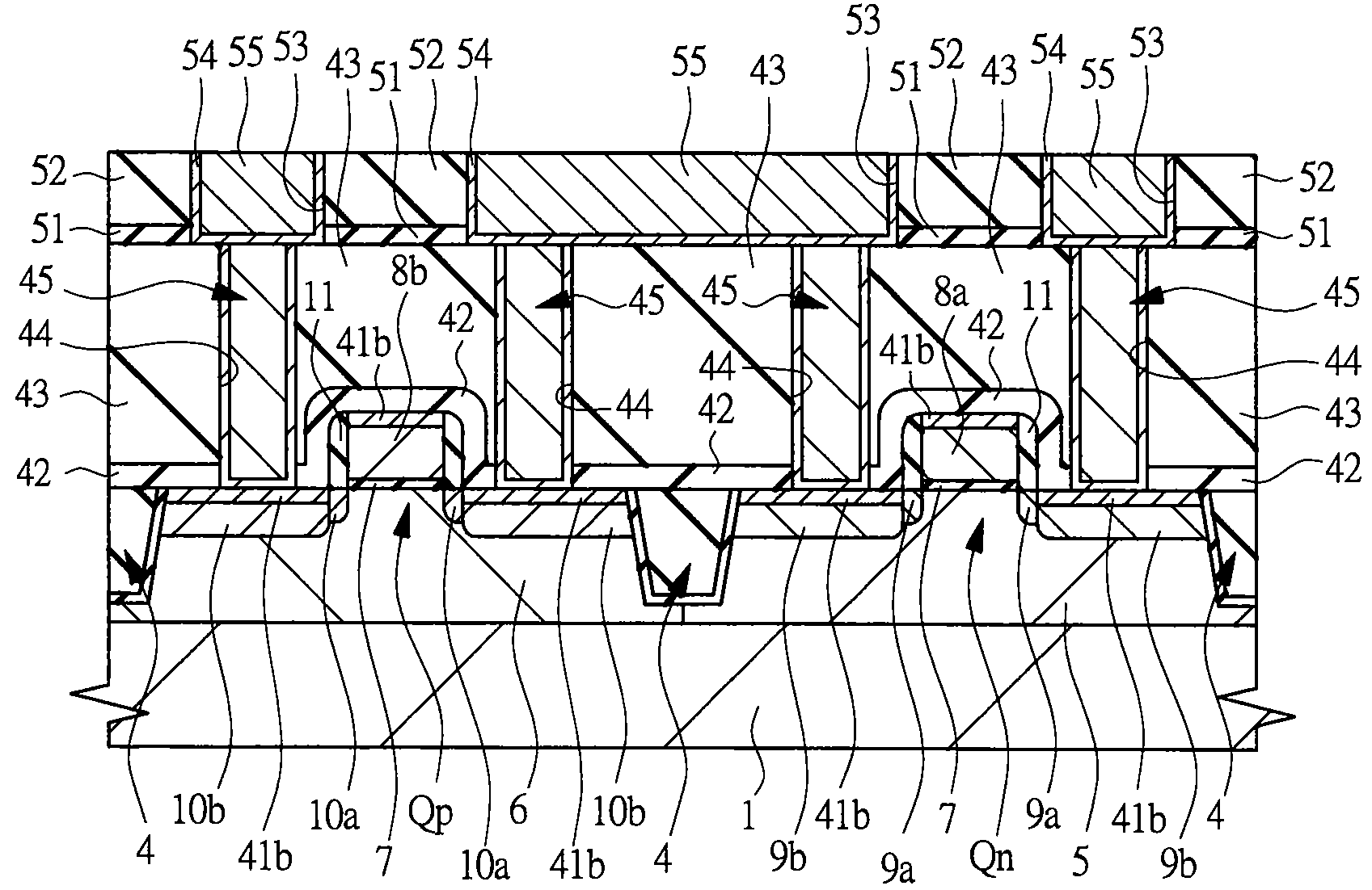
[0258]FIG. 31 is a manufacturing process flow showing a part of the process of manufacturing a semiconductor device according to the present embodiment and corresponds to FIG. 9 of the above first embodiment. In FIG. 31, a manufacturing process flow in a process is shown where a metal silicide layer (metal / semiconductor reaction layer) is formed on the surface of gate electrodes 8a, 8b, n+ type semiconductor region 9b and p+ type semiconductor region 10b by salicide process after the structure of above FIG. 7 is obtained. FIG. 32 to FIG. 35 are cross-sectional views of main parts of the semiconductor device in the manufacturing process of the present embodiment.

[0259]The process of manufacturing the semiconductor device according to the present embodiment is same to the process of the above first embodiment until the process in which wet cleaning is carried out in the above step S4, and thereby the barrier film 13 and the unreacted metal film 12 are removed. Therefore, the explanati...

third embodiment

[0274]In a further study on the process of the comparative example of above described FIG. 18 to FIG. 21, the inventors have found that, in the source / drain of a p-channel type MISFET, the increase of the junction leakage current and the unevenness of the junction leakage current (the change of the junction leakage current in every transistor) are more likely to occur than in an n-channel type MISFET.

[0275]To reduce the above junction leakage current, it is effective to thin the thickness of Ni film 112 to be deposited on the semiconductor substrate 1 so that the thickness of nickel silicide layer 141b is thinned. However, the nickel silicide layer 141b is arranged for lowering resistance. Therefore, if the thickness of the nickel silicide layer 141b is made thin in both of the n-channel type MISFET and the p-channel type MISFET, the effect of lowering resistance by the nickel silicide layer 141b is weakened even in the n-channel type MISFET in which influence is hardly occurred to ...


PUM

PropertyMeasurementUnit
temperatureaaaaaaaaaa

Abstract

After gate insulating films, gate electrodes, and n+ type semiconductor regions and p+ type semiconductor regions for source / drain are formed, a metal film and a barrier film are formed on a semiconductor substrate. And a first heat treatment is performed so as to make the metal film react with the gate electrodes, the n+ type semiconductor region, and the p+ type semiconductor region, thereby forming a metal silicide layer formed of a monosilicide of a metal element forming the metal film. After that, the barrier film and the unreacted metal film are removed, and then a second heat treatment is performed to stabilize the metal silicide layer. The heat treatment temperature is made lower than a temperature at which a lattice size of a disilicide of the metal element and that of the semiconductor substrate become same.

Description

CROSS-REFERENCE TO RELATED APPLICATION[0001]The present application claims priority from Japanese Patent Application No. JP 2007-175501 filed on Jul. 3, 2007, Japanese Patent Application No. JP 2007-182031 filed on Jul. 11, 2007, and Japanese Patent Application No. JP 2008-106606 filed on Apr. 16, 2008, the contents of which are hereby incorporated by reference into this application.TECHNICAL FIELD OF THE INVENTION[0002]The present invention relates to a method of manufacturing a semiconductor device. More particularly, it relates to a technology effectively applied to manufacture of a semiconductor element comprising a metal silicide layer.BACKGROUND OF THE INVENTION[0003]As the high integration of semiconductor devices has been progressed, a field effect transistor (MISFET: Metal Insulator Semiconductor Field Effect Transistor) has been miniaturized according to the scaling law. However, a problem rises that the resistances of the gate and source / drain are increased, and high-spee...

Claims


Application Information

Patent Timeline
Patent Type & Authority Applications(United States)
IPC IPC(8): H01L21/44H01L21/336
CPCH01L21/0206H01L21/28518H01L21/324H01L29/7833H01L21/76224H01L29/665H01L29/6659H01L21/67184H01L21/24
Inventor OKADA, SHIGENARIFUTASE, TAKUYA
Owner RENESAS ELECTRONICS CORP
Why Eureka
Try Eureka