Sensing devices from molecular electronic devices
a technology of electronic devices and sensing devices, applied in the field of nanotube-based electronic devices, can solve the problems of difficult bonding between organic molecules and metal electrodes, difficult to select appropriate molecules, and difficult to achieve the effect of bonding
- Summary
- Abstract
- Description
- Claims
- Application Information
AI Technical Summary
Benefits of technology
Problems solved by technology
Method used
Image
Examples
example 1
Preparation of Contorted Hexabenzocoronenes
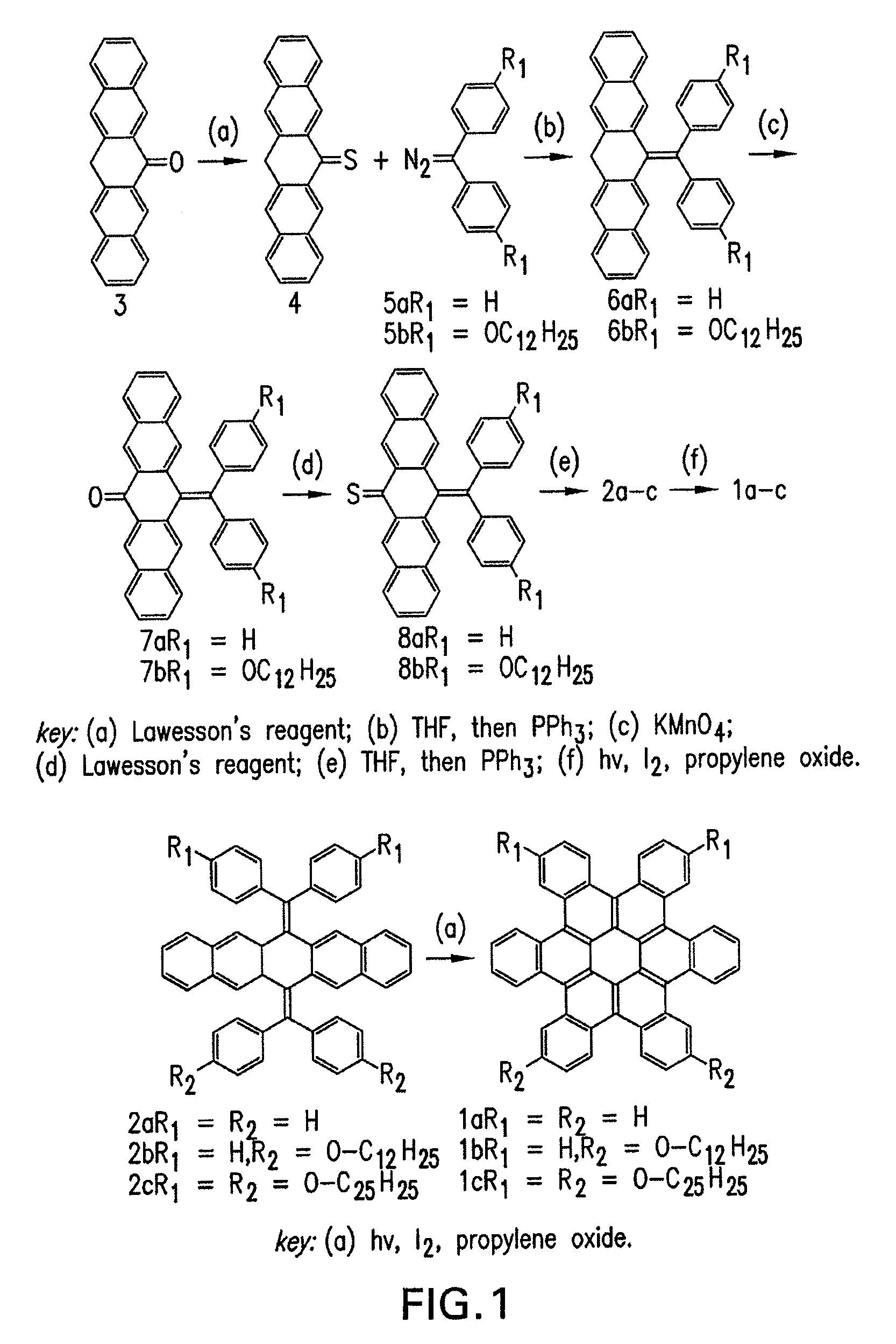
[0084]The syntheses for preparing contorted hexabenzocoronenes of formula 1 are schematically shown in FIG. 1. Ketone 3 was synthesized according to the well-known procedure disclosed in E. Clar, Chemische Berichte vol. 82, p. 495 (1949), the contents of which are incorporated by reference herein.
[0085]Synthesis of thioketone 4. Ketone 3 (4.4 g, 14.9 mmol) and Lawesson's reagent (0.7 eq, 4.2 g, 10.4 mmol) were added to 500 mL of toluene. The solution was heated to 80° C. for 2 hours. The dark green solution was allowed to cool to room temperature and 1200 mL of a 4:1 v / v mixture of hexanes and CH2Cl2 was added. Filtration through a plug of silica gel and a small amount of the same mixture of hexanes and CH2Cl2 was used to wash the remaining product from the silica gel. 3 was isolated as a green solid (2.2 g, 47%) after removal of the solvent and triturating with cold hexanes.
[0086]Synthesis of diphenyldiazomethane 5a: A mixture of 4,4′-dihy...
example 2
Preparation of a Transistor Device Based on Contorted HBCs
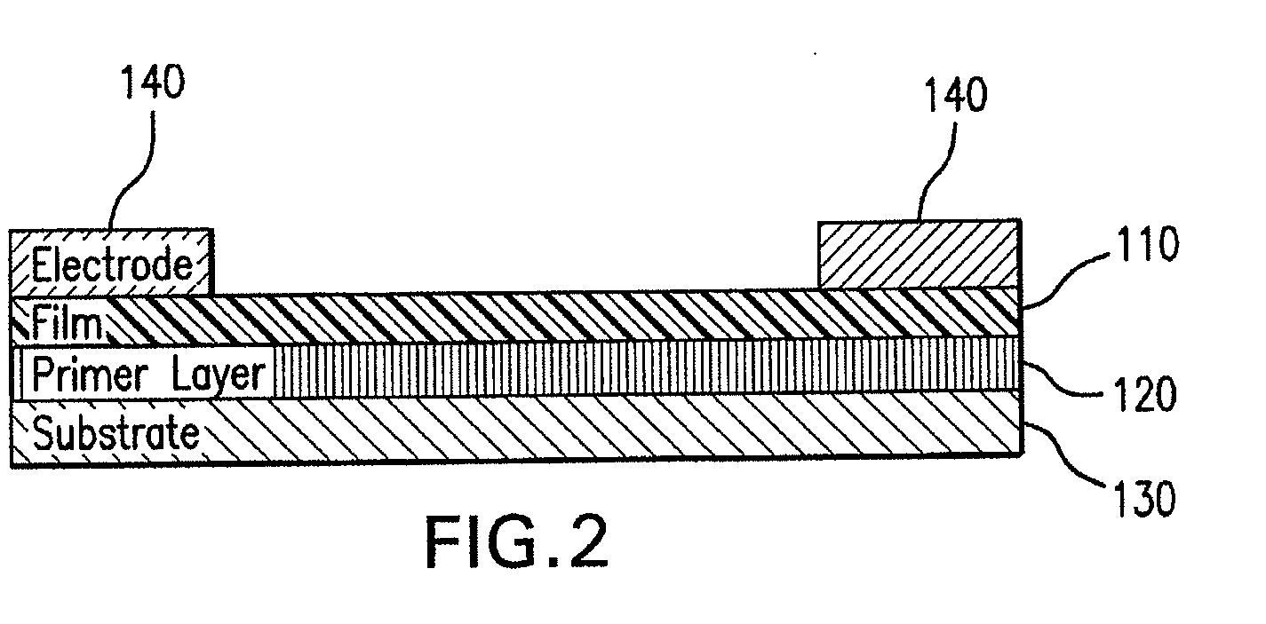
[0100]Compounds of the formula 1c were spin-cast from 1,2-dichloroethane or CHCl3 to form uniform films (approximately 100-nm thick) on top of a SiO2 substrate, and then Au was deposited as source and drain electrodes by thermal evaporation onto the spin-cast films through a metal-shadow mask. A transistor device thus obtained is illustrated schematically in FIG. 2. The transconductance and transistor output are shown in FIGS. 10A and 10B.
[0101]The mobility (0.02 cm2 V−1s−1) shown in FIG. 10B is calculated from the linear portion of the data in FIG. 10B, and was based on a capacitance of 11.3 nF cm−2 for the gate dielectric layer of 300 nm of SiO2 and a monolayer of octadecyltrichlorosilane, obtained from a series of measurements over a range of frequencies. Other critical parameters, such as the threshold voltage for the device to turn on (as low as −3 V) and the on / off current ratios in the device (106:1), are also very goo...
example 3
Fabrication of a Cut SWNT-Film Transistor Device
[0106]A compound of the formula 1c was spin cast onto the gap between a cut SWNT such that it covered gap of the cut SWNT but did not span the metal electrodes (shown in FIG. 15A). The device obtained shows p-type hole transporting semiconductor behavior (see FIG. 15B), but requires greater gate bias than a monolayer device where R2 is COCl is used where surface attachment is effected.
PUM
| Property | Measurement | Unit |
|---|---|---|
| diameters | aaaaa | aaaaa |
| RF power | aaaaa | aaaaa |
| temperature | aaaaa | aaaaa |
Abstract
Description
Claims
Application Information


