

Solid-state imaging element and method for fabricating the same
- Summary
- Abstract
- Description
- Claims
- Application Information
AI Technical Summary
Benefits of technology
Problems solved by technology
Method used
Image

Examples
embodiment 1
[0044]A solid-state imaging element and a method for fabricating the same according to the first embodiment of the present invention will be described.
[0045]First, a description will be given to a structure of the solid-state imaging element according to the first embodiment.
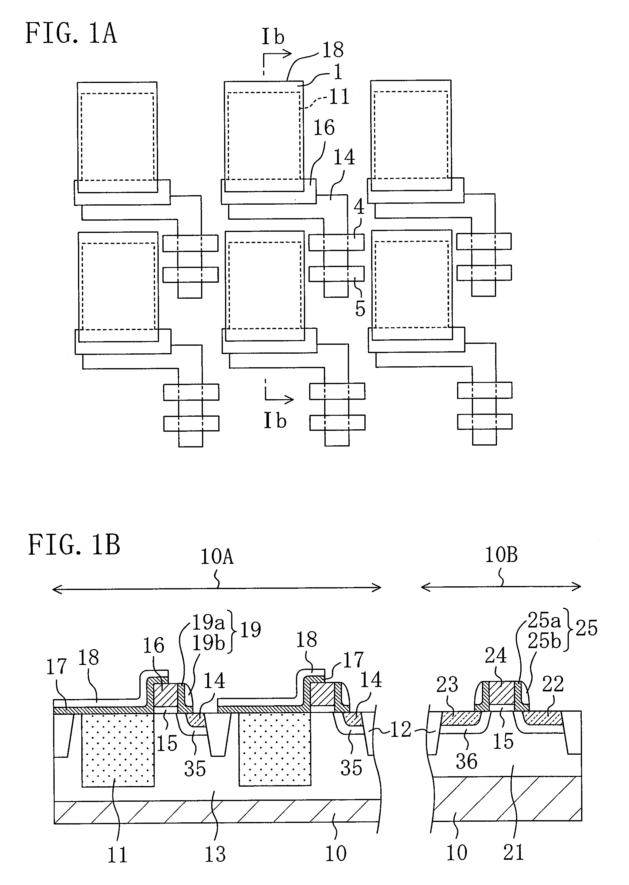
[0046]FIGS. 1A and 1B are views each showing the structure of the solid-state imaging element according to the first embodiment, specifically showing a CMOS image sensor as an example, of which 1A is a plan view, and FIG. 1B is a cross-sectional view corresponding to the line Ib-Ib of FIG. 1A.
[0047]In the plan view of FIG. 1A, the principal portion of the structure in which a plurality of pixels are arranged in an array is shown, and multilayer structures are formed. Each of the multilayer structures comprises an active region 1 including a photodiode 11 for performing a photoelectric conversion, a gate electrode 16 composing a transfer gate, a floating diffusion layer 14 made of an n-type diffusion layer, a gat...
embodiment 2
[0061]A solid-state imaging element and a method for fabricating the same according to the second embodiment of the present invention will be described.
[0062]First, a description will be given to a structure of the solid-state imaging element according to the second embodiment.
[0063]FIGS. 4A and 4B are views each showing a structure of the solid-state imaging element according to the second embodiment, specifically showing a CMOS image sensor as an example, of which 4A is a plan view, and FIG. 4B is a cross-sectional view corresponding to the line IVb-IVb of FIG. 4A.
[0064]The structure of the solid-state imaging element according to the present embodiment shown in FIGS. 4A and 4B is the same as that of the foregoing solid-state imaging element according to the first embodiment shown in FIGS. 1A and 1B, except that each of the silicon nitride films 18 has a different structure.
[0065]That is, as shown in FIGS. 4A and 4B, the structure of the solid-state imaging element according to th...
embodiment 3
[0072]A solid-state imaging element and a method for fabricating the same according to the third embodiment of the present invention will be described.
[0073]First, a description will be given to a structure of the solid-state imaging element according to the third embodiment.
[0074]FIGS. 6A and 6B are views each showing a structure of the solid-state imaging element according to the third embodiment, specifically showing a CMOS image sensor as an example, of which 6A is a plan view, and FIG. 6B is a cross-sectional view corresponding to the line VIb-VIb of FIG. 6A.
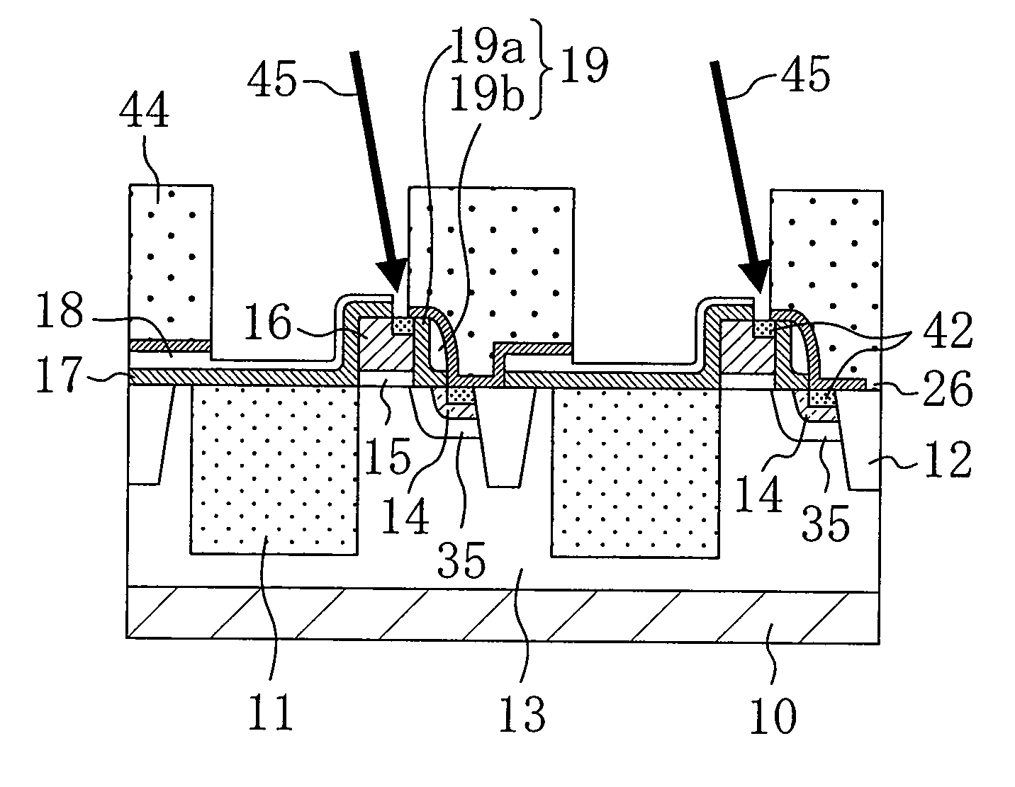
[0075]The structure of the solid-state imaging element according to the present embodiment shown in FIGS. 6A and 6B is the same as that of the foregoing solid-state imaging element according to the first embodiment shown in FIGS. 1A and 1B, except that a liner film 26 (not shown in FIG. 6A) made of a silicon nitride film formed over the entire surface of the silicon substrate 10 is further provided.
[0076]That is, as shown i...
PUM
 Abstract
Description
Claims
Application Information