Package structure of compound semiconductor device and fabricating method thereof

a technology of compound semiconductor and packaging structure, which is applied in the direction of semiconductor lasers, solid-state devices, semiconductor lasers, etc., can solve the problem of not being able to meet the requirements of high-power chemical compound semiconductor heat-transmission paths, and achieve the effect of improving the heat dissipation of the devi

Inactive Publication Date: 2009-01-22
ADVANCED OPTOELECTRONICS TECH
View PDF2 Cites 25 Cited by
  • Summary
  • Abstract
  • Description
  • Claims
  • Application Information

AI Technical Summary

Benefits of technology

[0008]One aspect of the present invention provides the package structure of a compound semiconductor device and fabricating method thereof. The semiconductor device has external electrodes or contacts uncovered by an encapsulation material. There is no printed circuit board between a die and external electrodes for transmitting electrical signals, so the heat dissipation of the device is improved.
[0009]Another aspect of the present invention provides the package structure of very thin semiconductor device and fabricating method thereof. The thickness of the device can be reduced for saving space because of the use of a thin substrate.

Problems solved by technology

On the other hand, the insulation layer 13c is made mostly of epoxy resin with poor heat dissipation, and therefore is not suitable for a high power chemical compound semiconductor as a heat-transferring path.

Method used


Image

  • Package structure of compound semiconductor device and fabricating method thereof
  • Package structure of compound semiconductor device and fabricating method thereof
  • Package structure of compound semiconductor device and fabricating method thereof

Examples


Embodiment Construction

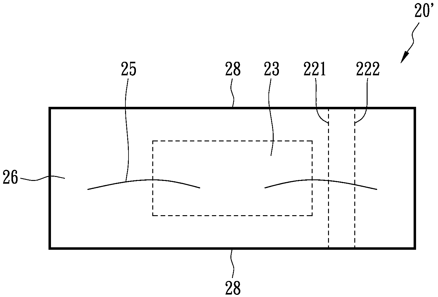
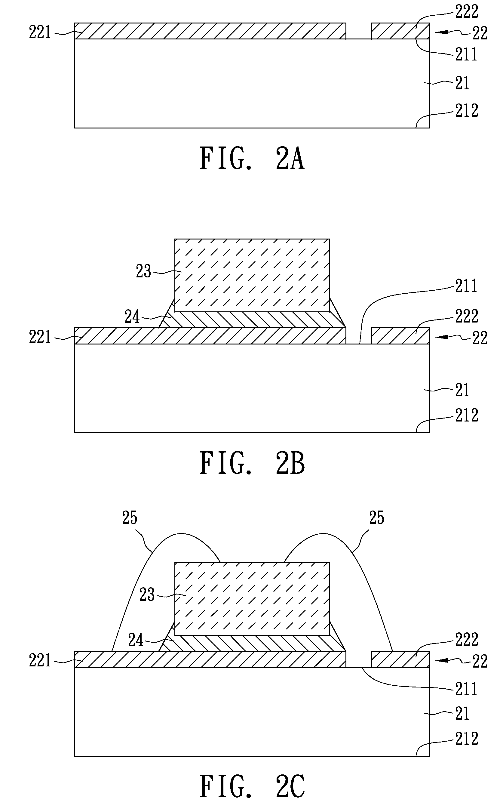
[0047]FIGS. 2A-2F are schematic illustrations showing the manufacturing steps of the package structure of a compound semiconductor device in accordance with the present invention. As shown in FIG. 2A, a temporary substrate 21 comprises a first surface 211 and a second surface 212. In this drawing, the first surface 211 is an upper surface and the second surface 212 is a lower surface. The temporary substrate 21 is made of a metallic material, a ceramic material and a polymer material. A conductive film 22 with a pattern is formed on the first surface 211 through printing, screening, electroform, chemical plating (or electroless plating) or sputtering. The material of the conductive film 22 is silver, nickel, copper, tin, aluminum or an alloy of the aforesaid metallic materials. Furthermore, indium tin oxide (ITO), indium zinc oxide (IZO), indium gallium oxide (IGO) and indium tungsten oxide (IWO) also are suitable for the material of the conductive film 22, and the film further comp...


PUM

PropertyMeasurementUnit
thicknessaaaaaaaaaa
thicknessaaaaaaaaaa
diameteraaaaaaaaaa

Abstract

A package structure of a compound semiconductor device comprises a thin conductive film with a pattern, a die, at least one metal wire or metal bump and a transparent encapsulation material. The die is mounted on the first surface of the thin conductive film, and is electrically connected to the thin conductive film through the metal wire or the metal bump. The transparent encapsulation material is overlaid on the first surface of the conductive film and the die. A second surface of the conductive film is not covered by the transparent encapsulation material, and is opposite the first surface.

Description

BACKGROUND OF THE INVENTION[0001](A) Field of the Invention[0002]The present invention relates to a package structure of a compound semiconductor device and fabricating method thereof, and more particularly, to a thin package structure and fabricating method of a photoelectric semiconductor device.[0003](B) Description of the Related Art[0004]Because the light emitting diode (LED) pertaining to the photoelectric device has advantages of a small body, high efficiency and long lifetime, it is deemed as an excellent illuminant source for the next generation. Furthermore, LCD (liquid crystal display) technology is developing rapidly and full color is the current trend in electronic product displays. Therefore, the white series LEDs are not only applicable to indication lights and large size display screens but also to most consumer electronic products such as mobile phones and personal digital assistants (PDA).[0005]FIG. 1 is a schematic cross sectional diagram of the conventional SMD (...

Claims


Application Information

Patent Timeline
Patent Type & Authority Applications(United States)
IPC IPC(8): H01S5/028H01L33/00H01L31/18H01L31/0232H01L33/50H01L33/56H01L33/60H01L33/62H01L33/64
CPCH01L31/0203H01L31/18H01L2924/01322H01L2224/92247H01L2224/73265H01L2224/48247H01L2224/32245H01L2224/16245H01L2224/48091H01L33/54H01L33/486H01L2924/00H01L2924/00012H01L2924/00014H01L24/73
Inventor CHEN, PIN CHUANCHANG, CHAO HSIUNGLIN, SHEN BOCHEN, LUNG HSINTSENG, WEN LIANG
Owner ADVANCED OPTOELECTRONICS TECH
Why Eureka
Try Eureka