Method for fabricating dual damascene profiles using sub pixel-voting lithography and devices made by same

a technology of damascene and lithography, which is applied in the direction of photomechanical treatment originals, instruments, photomechanical equipment, etc., can solve the problems of not being significantly implemented in the main stream manufacturing of semiconductor devices, requiring a significant number of discrete processing steps, and employing a complex fabrication sequence, so as to reduce the complexity, reduce the cost associated, and improve the effect of throughpu

Active Publication Date: 2009-01-22
THE BOARD OF TRUSTEES OF THE UNIV OF ILLINOIS
View PDF60 Cites 30 Cited by
  • Summary
  • Abstract
  • Description
  • Claims
  • Application Information

AI Technical Summary

Benefits of technology

[0064]An advantage of the present invention is that it makes use of a single layer of resist. This advantage not only reduces the complexity in making the above mentioned profiles but also significantly reduces the costs associated with purchasing additional resists and developers for the resists. The present methods also improve throughput because both trenches and vias are etched in the same step. The present methods are particularly attractive for Dual Damascene processing because not only are the trenches and vias simultaneously deposited with metal but they are also simultaneously etched.
[0065]Specific embodiments of the present invention are further described and set forth by reference to the Figures.
[0066]FIG. 1 illustrates the use of overlapping exposure of selected areas of a resist layer for making Dual Damascene integrated trench and via features and embedded multilevel interconnect structures. The exposure areas exemplified in FIGS. 1A and 1B correspond to areas of a resist layer provided on a substrate undergoing processing that are exposed to radiation (as shown in FIG. 2). FIG. 1A illustrates the dimensions and shape of a first area of the resist layer exposed to a selected intensity of radiation comprising rectangle 1, and the dimensions and shape of a second area of the resist layer exposed to radiation comprising square 2. FIG. 1B shows the spatial arrangement of rectangle 1 and square 2 useful for making recessed features and embedded structures having a non-uniform cross sectional profile. As shown in FIG. 1B, the exposed first and second areas are positioned so as to provide overlap between rectangle 1 and square 2. Specifically, square 2 is positioned such that it entirely overlaps rectangle 1, as shown in FIG. 1B. This overlap configuration is particularly useful for making a recessed feature in the substrate corresponding to a Dual Damascene profile comprising integrated trench and via features.
[0067]In a specific embodiment, rectangle 1 and square 2 are both patterned in the resist layer using a 50% dose of radiation, and are positioned to overlap in the manner shown in FIG. 1B. Although a 50% does is exemplified, any sub-threshold dose is useable in this specific embodiment of the present invention. Overlapping region 3 corresponds to the entire area square 2, as shown in FIG. 1B, and as a result of the overlap of rectangle 1 and square 2, overlapping region 3 is exposed to a cumulative intensity of radiation corresponding to a 100% dose radiation. Once lithographic patterning via exposure of rectangle 1 and square 2 to selected intensities of radiation is completed, the patterned resist layer is subsequently developed so as to generate a recessed feature in the layer of resist having a non-uniform depth profile (See, e.g., FIG. 2).
[0068]FIG. 2 provides a schematic illustrating additional processing steps of methods of the present invention, including development, transfer, stripping and deposition steps. FIG. 2A provides a cross sectional view of the resist layer 5 provided on the substrate 4 undergoing processing. As discussed in the context of FIG. 1, resist layer 5 is lithographically patterned using overlapping exposure of rectangle 1 and square 2. FIG. 2B shows a cross sectional view the resist layer 5 and substrate 4 upon developing the patterned resist layer 5. As shown in FIG. 2B, developing removes material from the patterned resist layer 5 in first and second areas exposed to radiation. Development may be carried out by any means known in the art including via dissolution using developers and developing agents.
[0069]As shown in FIG. 2B, the non-overlapping area of the first exposed area corresponding rectangle 1 that received a net 50% dose of radiation is reduced to a half or lower than half of the original thickness due to incomplete removal of resist during developing. In contrast, the overlapping area 3, corresponding to square 2 provided in an entirely overlapping configuration, undergoes complete development and, hence, resist is completely removed along the entire thickness of the resist layer 5 in a region corresponding to the overlapping area. As a result of development, therefore, a region 6a of the substrate 4 is exposed corresponding to the overlapping area of patterned first and second areas. The result of developing, as shown in FIG. 2B, is generation of a recessed feature 6 in the resist layer 5 having a non-uniform, T-shaped depth profile.

Problems solved by technology

Although current Dual Damascene approaches reduce the total number of processing steps required to make complex multilevel interconnect structures, this fabrication technique still requires a significant number of discrete processing steps (e.g., 20-30) per layer of a multilayer electronic device.
This process employs a complex fabrication sequence relative to Trench First and Via First processes, however, and is currently not significantly implemented for main stream manufacturing of semiconductor devices.
First, use of multiple resist processing steps adds considerably to the cost of commercial implementation, as the overall cost of semiconductor device fabrication increases at an exponential rate with the number of resist deposition, patterning developing steps in a given process.
Second, Trench First and Via First Dual Damascene require two separate anisotropic etch processing sequences which decreases overall throughput and also significantly increases cost of this fabrication method.
Since the resist is commonly in the liquid phase it fills the trench structures etched into the outermost dielectric layer, and therefore, commonly does not form a uniform layer of photoresist if applied too thin.
In order to get a uniform coating, the resist layer commonly needs to be very thick, which commonly impedes forming very fine and / or high resolution features of the via structures in the dielectric material.
The single photoresist processing strategies described in U.S. Pat. Nos. 6,355,399 and 5,976,968 lack processing flexibility, however, and also require a large photomask library for commercial implementation.

Method used


Image

  • Method for fabricating dual damascene profiles using sub pixel-voting lithography and devices made by same
  • Method for fabricating dual damascene profiles using sub pixel-voting lithography and devices made by same
  • Method for fabricating dual damascene profiles using sub pixel-voting lithography and devices made by same

Examples


example 1

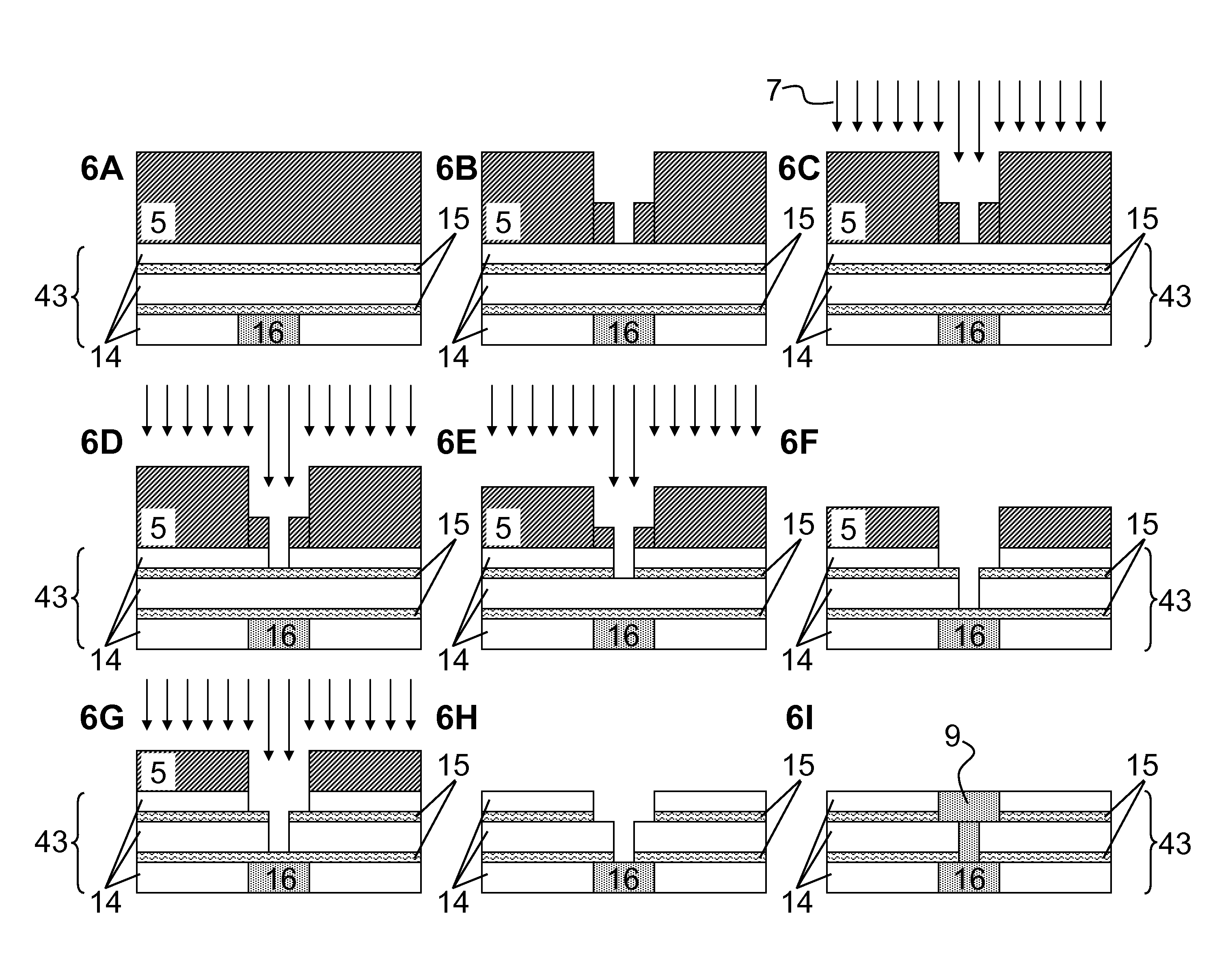
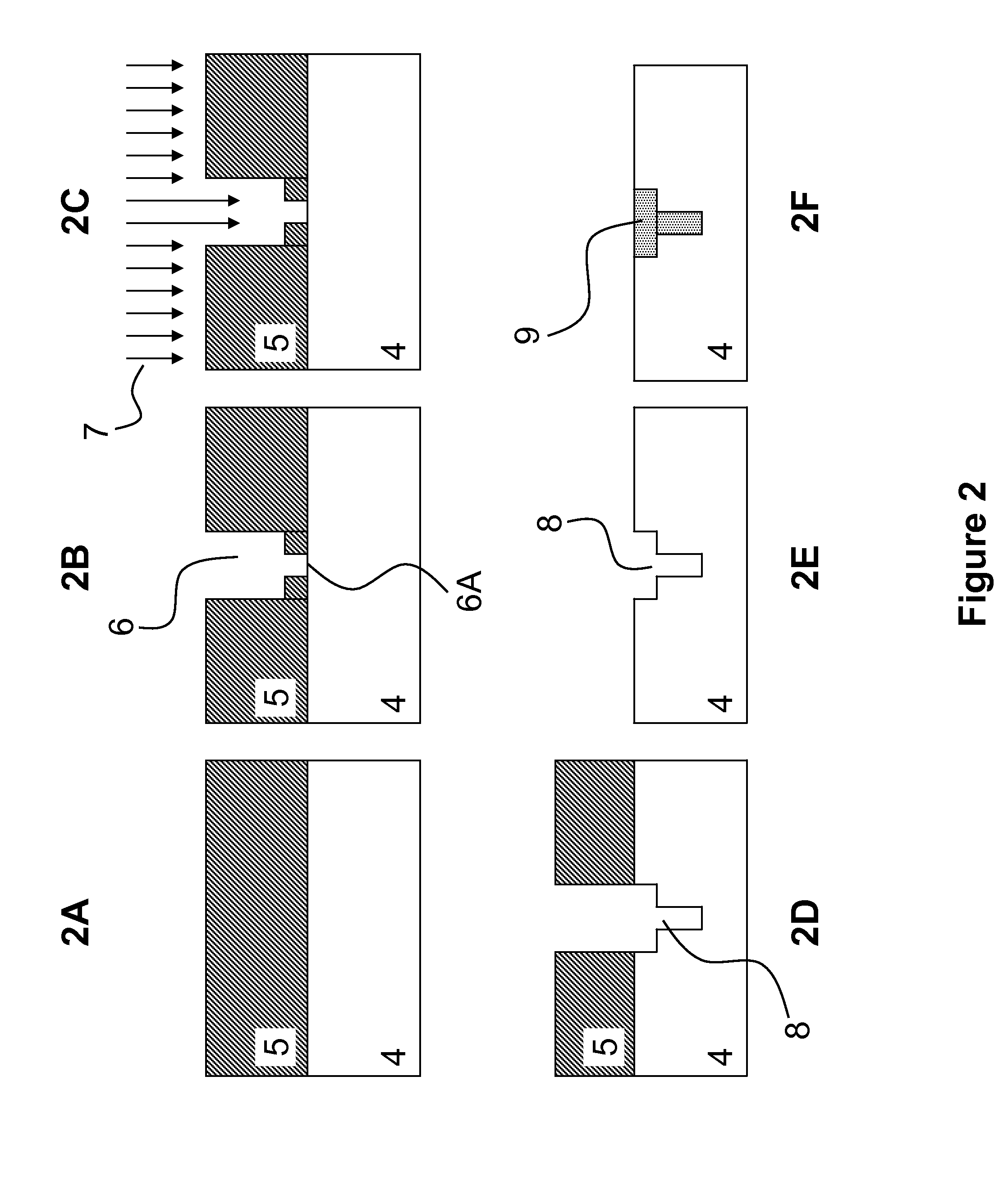
Method of Making a Dual Damascene Profile

[0086]To demonstrate the capability of present methods using partial exposures to pattern Dual Damascene profiles for making Dual Damascene profiles, e-beam lithography was used for generating an overlapping exposure of a resist layer to radiation. A two inch silicon wafer was used as the substrate in our process. Silicon dioxide of thickness 200 nm was deposited on the silicon surface by PEVCD. In our experiments we did not deposit any etch stop materials in order to avoid unnecessary processing complexity. Once the wafer was cleaned with solvents, 260 nm of 950,000 4% in Anisole, PMMA was deposited on the substrate. Specifically, a 2600 Å layer of PMMA was spun onto the wafer. Once the resist was applied, the sample was heated to 200° C. in order to drive out any remaining solvent.

[0087]We then expose the substrate to an E-Beam, which first writes a rectangle at a dose of 50%. The rectangle has a width of 2 um. We then pattern a square of s...


PUM

PropertyMeasurementUnit
areaaaaaaaaaaa
areaaaaaaaaaaa
areaaaaaaaaaaa

Abstract

This invention provides processing steps, methods and materials strategies for making patterns of structures for integrated electronic devices and systems. Processing methods of the present invention are capable of making micro-and nano-scale structures, such as Dual Damascene profiles, recessed features and interconnect structures, having non-uniform cross-sectional geometries useful for establishing electrical contact between device components of an electronic device. The present invention provides device fabrication methods and processing strategies using sub pixel-voting lithographic patterning of a single layer of photoresist useful for fabricating and integrating multilevel interconnect structures for high performance electronic or opto-electronic devices, particularly useful for Very Large Scale Integrated (VLSI) and Ultra large Scale Integrated (ULSI) devices. Processing methods of the present invention are complementary to conventional microfabrication and nanofabrication methods for making integrated electronics, and can be effectively integrated into existing photolithographic, etching, and thin film deposition patterning systems, processes and infrastructure.

Description

CROSS-REFERENCE TO RELATED APPLICATIONS[0001]This application claims priority under 35 U.S.C. 119(e) to U.S. provisional Patent Application 60 / 950,020 filed Jul. 16, 2007, which is hereby incorporated by reference in its entirety to the extent not inconsistent with the present description.STATEMENT REGARDING FEDERALLY SPONSORED RESEARCH OR DEVELOPMENT[0002]Not applicable.BACKGROUND OF INVENTION[0003]Consumer demand for electronic devices capable of high operating speeds continues to provide significant motivation for the development of integrated circuits capable of enhanced device performance. Advanced lithographic and direct writing patterning techniques, for example, currently enable microprocessor designs having large scale integration of 10s to 100s of millions of microsized device components in dense multilevel configurations. Critical to practical implementation of such high density device geometries, however, is the development of interconnect structures capable of establish...

Claims


Application Information

Patent Timeline
Patent Type & Authority Applications(United States)
IPC IPC(8): G03F7/20G03F7/22
CPCH01L21/0277H05K3/107H01L21/31144H01L21/76807H01L21/76813Y10T428/24612H01L2221/1021
Inventor JAIN, KANTIREDDY, UTTAM
Owner THE BOARD OF TRUSTEES OF THE UNIV OF ILLINOIS
Why Eureka
Try Eureka