Manufacturing method of soi substrate

a manufacturing method and soi technology, applied in the direction of basic electric elements, electrical apparatus, semiconductor devices, etc., can solve the problems of brittleness of the ion implantation membrane layer, and achieve the effect of increasing productivity, increasing throughput, and increasing productivity of the semiconductor device which uses the soi substra

Inactive Publication Date: 2009-01-29
SEMICON ENERGY LAB CO LTD
View PDF60 Cites 43 Cited by
  • Summary
  • Abstract
  • Description
  • Claims
  • Application Information

AI Technical Summary

Benefits of technology

[0019]The present invention provides a manufacturing method of an SOI substrate with higher throughput, thereby increasing productivity. Further, productivity of a semiconductor device which uses an SOI substrate can also be increased.

Problems solved by technology

In addition, “the progression of embrittlement” means that the number of voids formed is increased, the voids become larger, or the voids are bonded to each other, thereby forming a space to partially separate a semiconductor substrate; that is, “the progression of embrittlement” means that an embrittlement layer formed by ion implantation becomes more brittle than what it used to be.

Method used


Image

  • Manufacturing method of soi substrate
  • Manufacturing method of soi substrate
  • Manufacturing method of soi substrate

Examples


embodiment mode 1

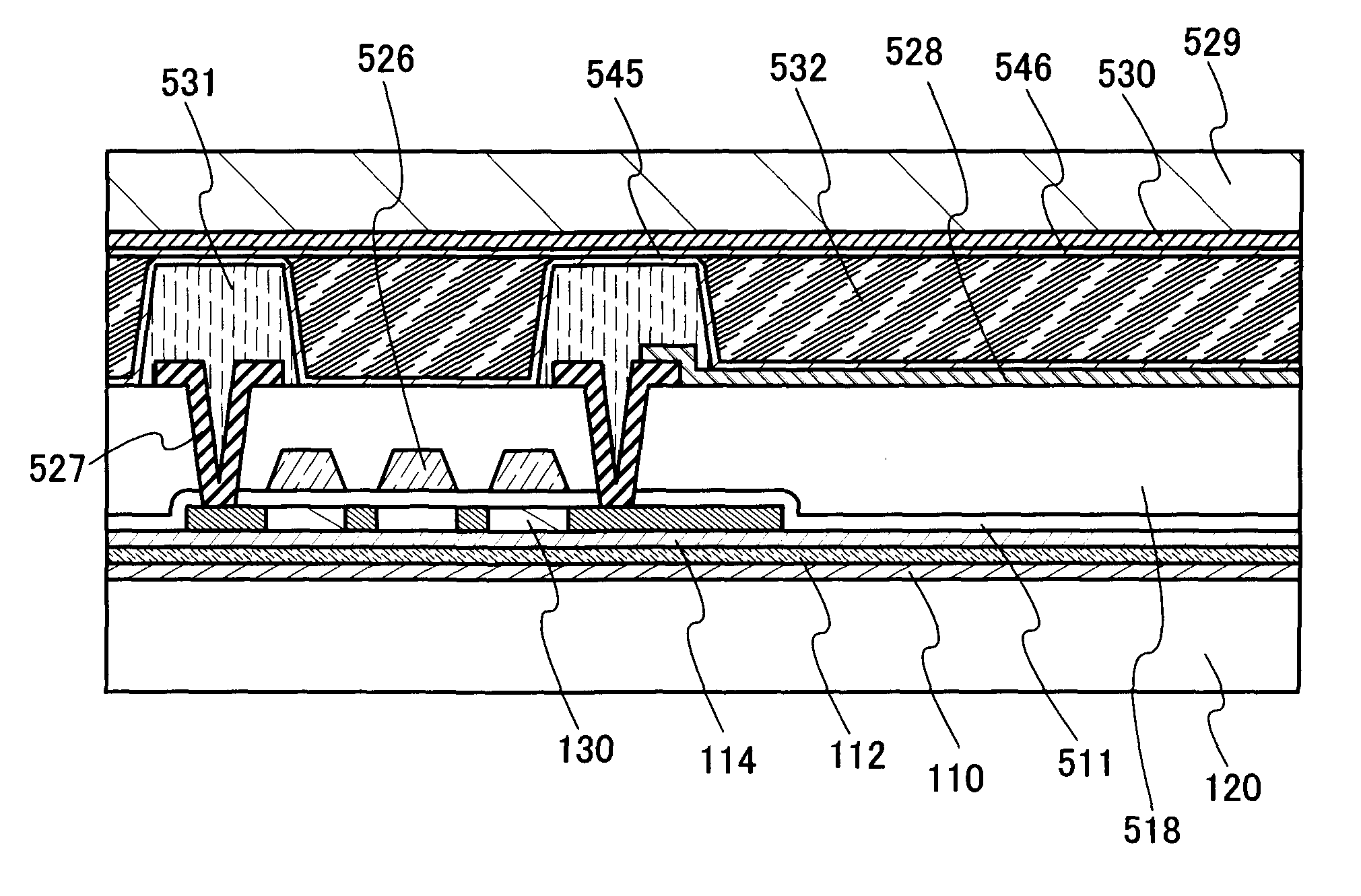
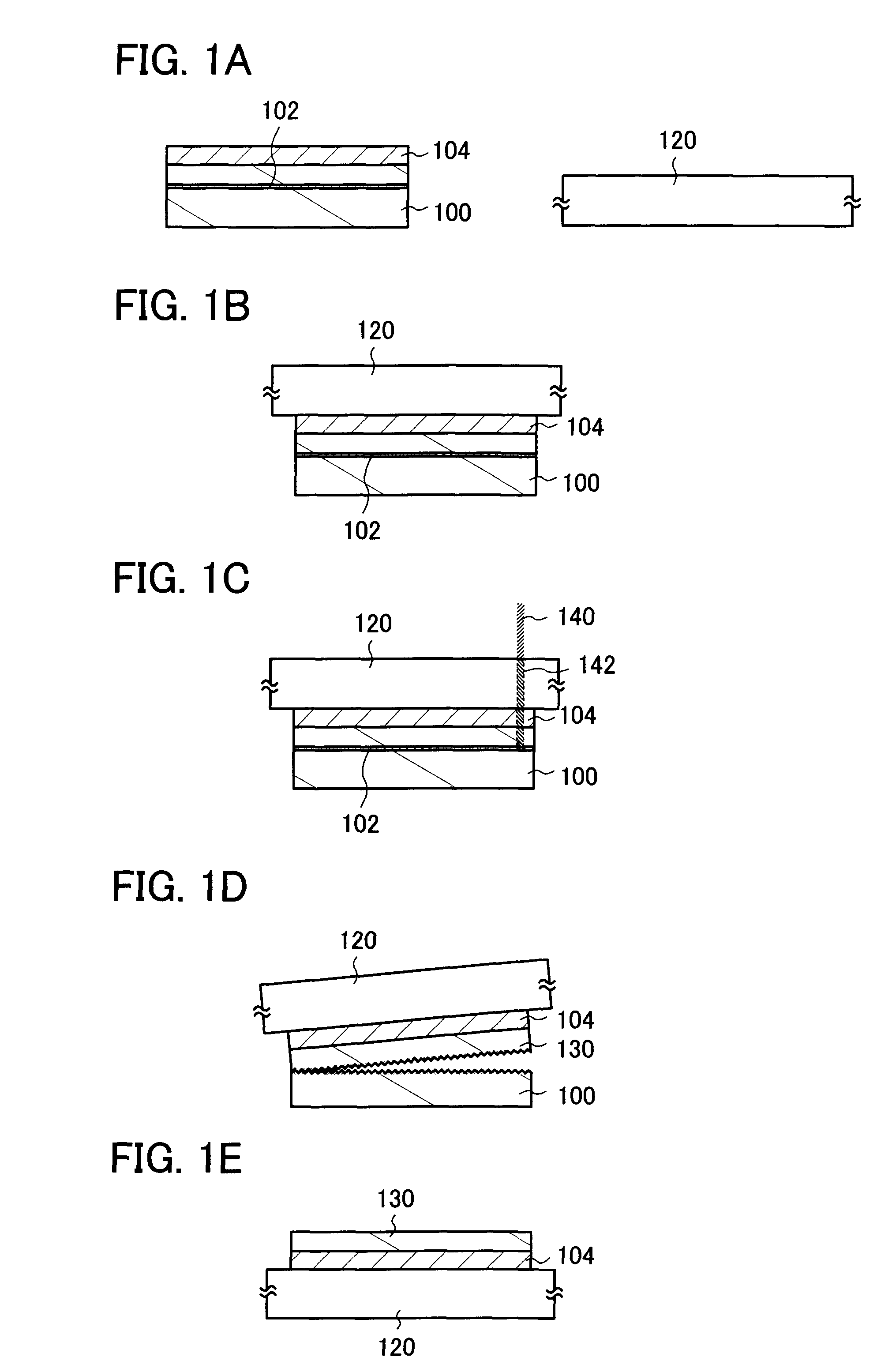
[0051]An SOI substrate of this embodiment mode is formed by transferring a semiconductor layer separated from a semiconductor substrate, preferably a single-crystalline semiconductor layer separated from a single-crystalline semiconductor substrate, to a supporting substrate. As the supporting substrate, a different kind of substrate from the semiconductor substrate is used. An example of a manufacturing method of an SOI substrate according to this embodiment mode will be described below with reference to the drawings.

[0052]A semiconductor substrate 100 which includes an embrittlement layer 102 in a region at a predetermined depth and on a surface of which an insulating layer 104 is formed, and a supporting substrate 120 are prepared (see FIG. 1A).

[0053]As the semiconductor substrate 100, a semiconductor substrate such as a silicon substrate or a germanium substrate, or a compound semiconductor substrate such as a gallium arsenide substrate or an indium phosphide substrate is used. ...

embodiment mode 2

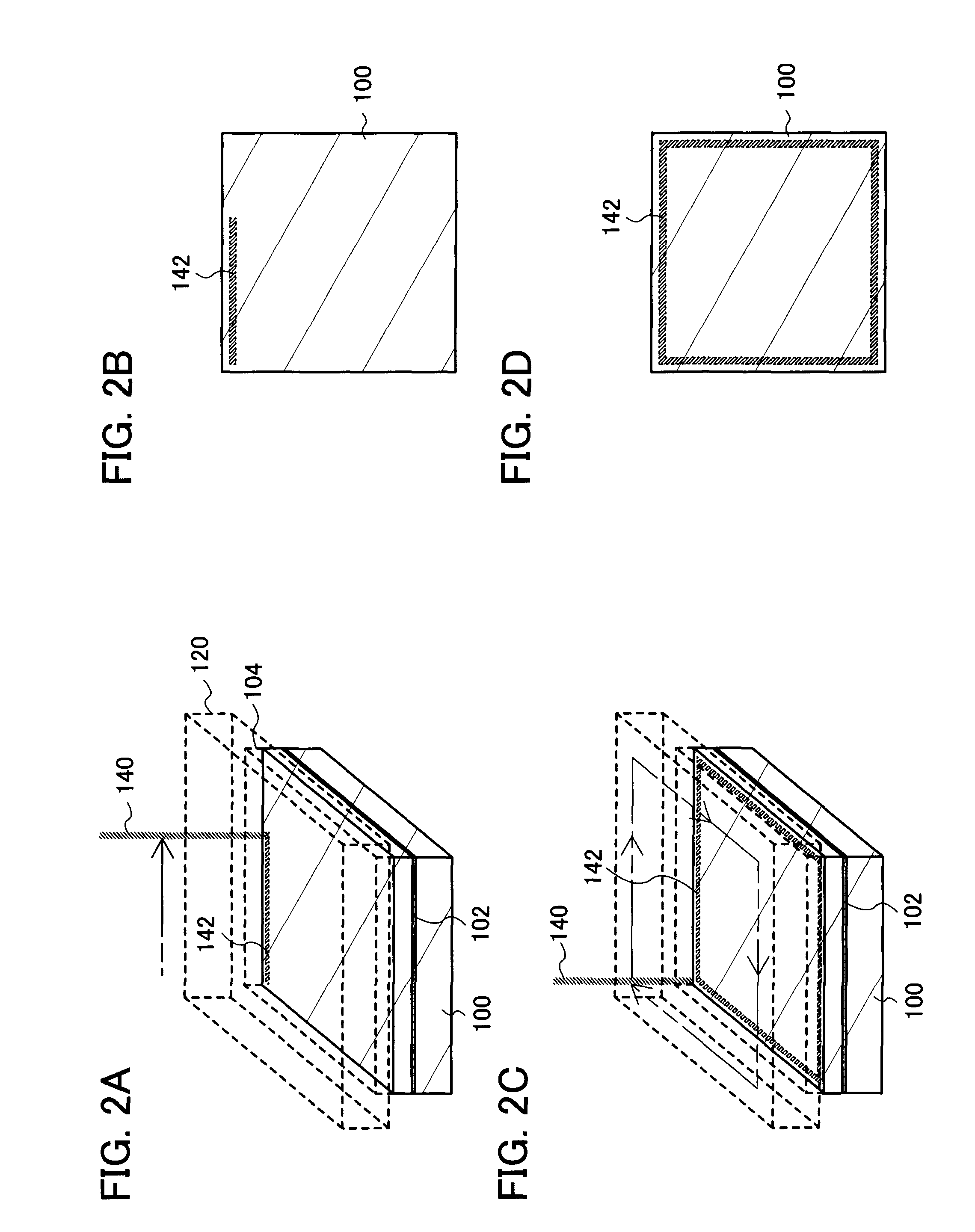
[0116]Although the example in which irradiation with a laser beam is performed from the supporting substrate direction is described in the above embodiment mode, an example of directly irradiating a semiconductor substrate with a laser beam will be described in Embodiment Mode 2 with reference to FIGS. 6A and 6B.

[0117]FIGS. 6A and 6B are schematic perspective views illustrating a semiconductor substrate 100 and a supporting substrate 120 which are bonded to each other with an insulating layer 104 interposed therebetween. An embrittlement layer 102 is formed in a region at a predetermined depth of the semiconductor substrate 100. With regard to the semiconductor substrate 100, the embrittlement layer 102, the supporting substrate 120, and the insulating layer 104, refer to description of those in Embodiment Mode 1. Further, in FIGS. 6A and 6B, the supporting substrate 120 and the insulating layer 104 are illustrated by dotted lines.

[0118]In this embodiment mode, side surfaces of the ...

embodiment mode 3

[0126]In Embodiment Mode 3, a manufacturing method of an SOI substrate, which is different from those in the above embodiment modes will be described.

[0127]A semiconductor substrate 100 which includes an embrittlement layer 102 in a region at a predetermined depth and on a surface of which an insulating layer 104 is formed, and a supporting substrate 120 are prepared. Then, the semiconductor substrate 100 and the supporting substrate 120 are bonded to each other with the insulating layer 104 interposed therebetween. Next, selective irradiation with a laser beam 140 is performed from the supporting substrate 120 side to make embrittlement of an embrittlement layer 102 progress partially (see FIG. 7A).

[0128]In this embodiment mode, the formation order of the embrittlement layer 102 and the insulating layer 104 is not limited. After formation of the embrittlement layer 102 by irradiating the semiconductor substrate 100 with ions, the insulating layer 104 may be formed. Alternatively, a...


PUM


Abstract

A manufacturing method of an SOI substrate with high throughput. A semiconductor layer separated from a semiconductor substrate is transferred to a supporting substrate, thereby manufacturing an SOI substrate. First, the semiconductor substrate serving as a base of the semiconductor layer is prepared. An embrittlement layer is formed in a region at a predetermined depth of the semiconductor substrate, and an insulating layer is formed on a surface of the semiconductor substrate. After bonding the semiconductor substrate and a supporting substrate with the insulating layer interposed therebetween, the semiconductor substrate is selectively irradiated with a laser beam; accordingly, embrittlement of the embrittlement layer progresses. Then, using a physical method or heat treatment, the semiconductor substrate is separated; at that time, the region where the embrittlement has progressed in the embrittlement layer serves as a starting point.

Description

BACKGROUND OF THE INVENTION[0001]1. Field of the Invention[0002]The present invention relates to an SOI (silicon on insulator) substrate and a manufacturing method thereof.[0003]Note that a semiconductor device in this specification refers to all types of devices which can function by utilizing semiconductor characteristics, and electro-optic devices, semiconductor circuits, and electronic devices are all included in the category of the semiconductor device.[0004]2. Description of the Related Art[0005]With development of VLSI technology, lower power consumption and higher speed over the scaling law which can be realized by bulk single-crystalline silicon have been demanded. In order to satisfy these requirements, an SOI structure is receiving attention. This technology allows an active region (channel formation region) of a field effect transistor (FET), which has been formed of bulk single-crystalline silicon, to be formed of a single-crystalline silicon thin film. It is known that...

Claims


Application Information

Patent Timeline
Patent Type & Authority Applications(United States)
IPC IPC(8): H01L21/30
CPCH01L21/76254H01L29/42384H01L27/1266H01L29/78621H01L29/78603
Inventor OHNUMA, HIDETO
Owner SEMICON ENERGY LAB CO LTD
Why Eureka
Try Eureka