Semiconductor Device and Method of Manufacturing the Semiconductor Device

a semiconductor and semiconductor technology, applied in semiconductor devices, instruments, optics, etc., can solve problems such as complicated work, and achieve the effect of improving yield and reducing manufacturing costs

Inactive Publication Date: 2009-02-05
SEMICON ENERGY LAB CO LTD
View PDF97 Cites 190 Cited by
  • Summary
  • Abstract
  • Description
  • Claims
  • Application Information

AI Technical Summary

Benefits of technology

[0008]The present invention has been made in order to solve the above problems, and therefore an object of the present invention is to realize a reduction of the manufacturing costs and an improvement of the yield by reducing the number of processes for manufacturing the TFTs in an electro-optical device and a semiconductor device which are represented by an active matrix liquid crystal display device.

Problems solved by technology

Therefore, if one photomask is used, there added processes for resist coating, pre-baking, exposing, developing, post-baking, etc., processes for forming a film, etching, etc., which are conducted before and after the former processes and processes for separating the resist, cleaning and drying, etc., resulting in a complicated work.

Method used


Image

  • Semiconductor Device and Method of Manufacturing the Semiconductor Device
  • Semiconductor Device and Method of Manufacturing the Semiconductor Device
  • Semiconductor Device and Method of Manufacturing the Semiconductor Device

Examples


first embodiment

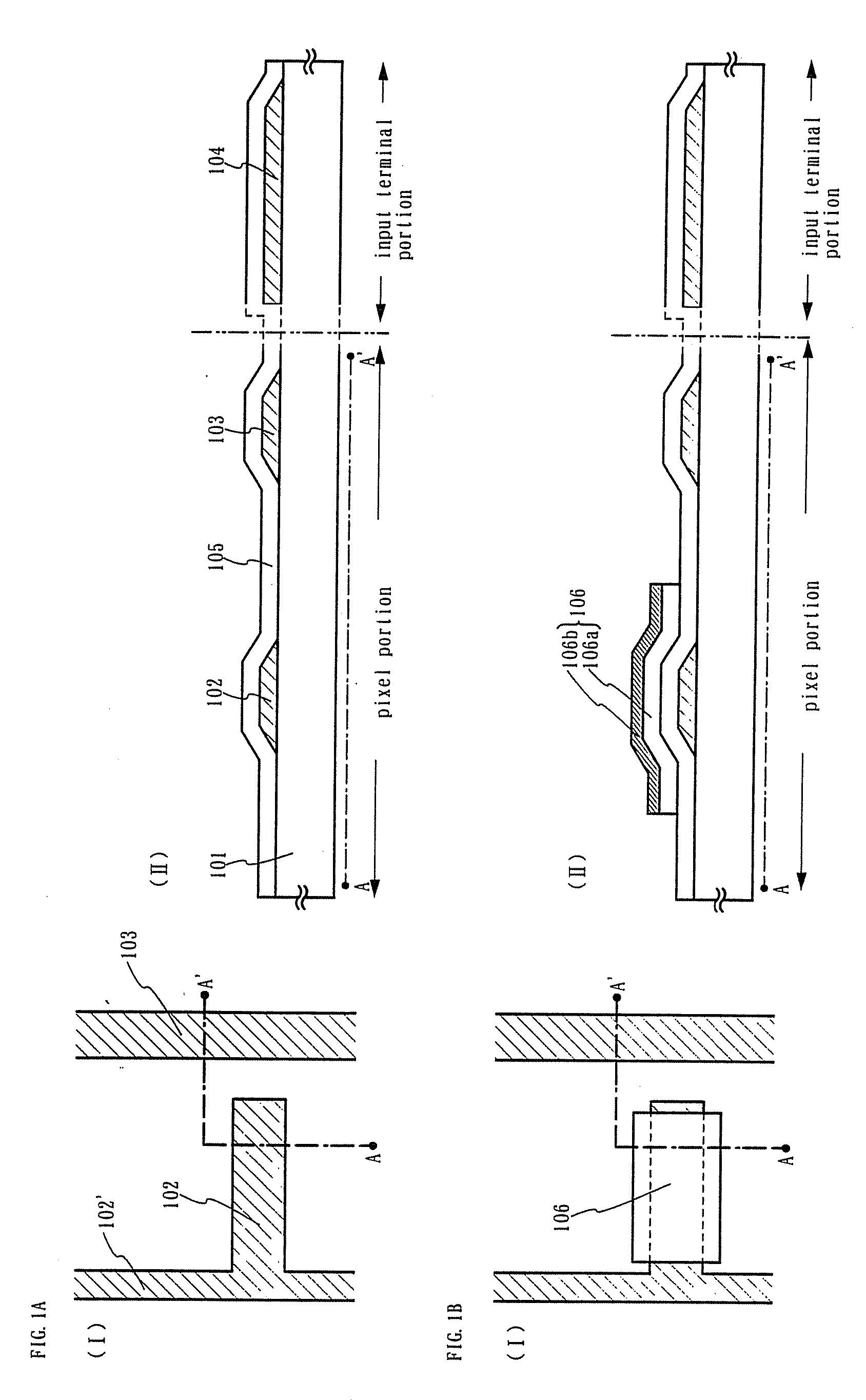
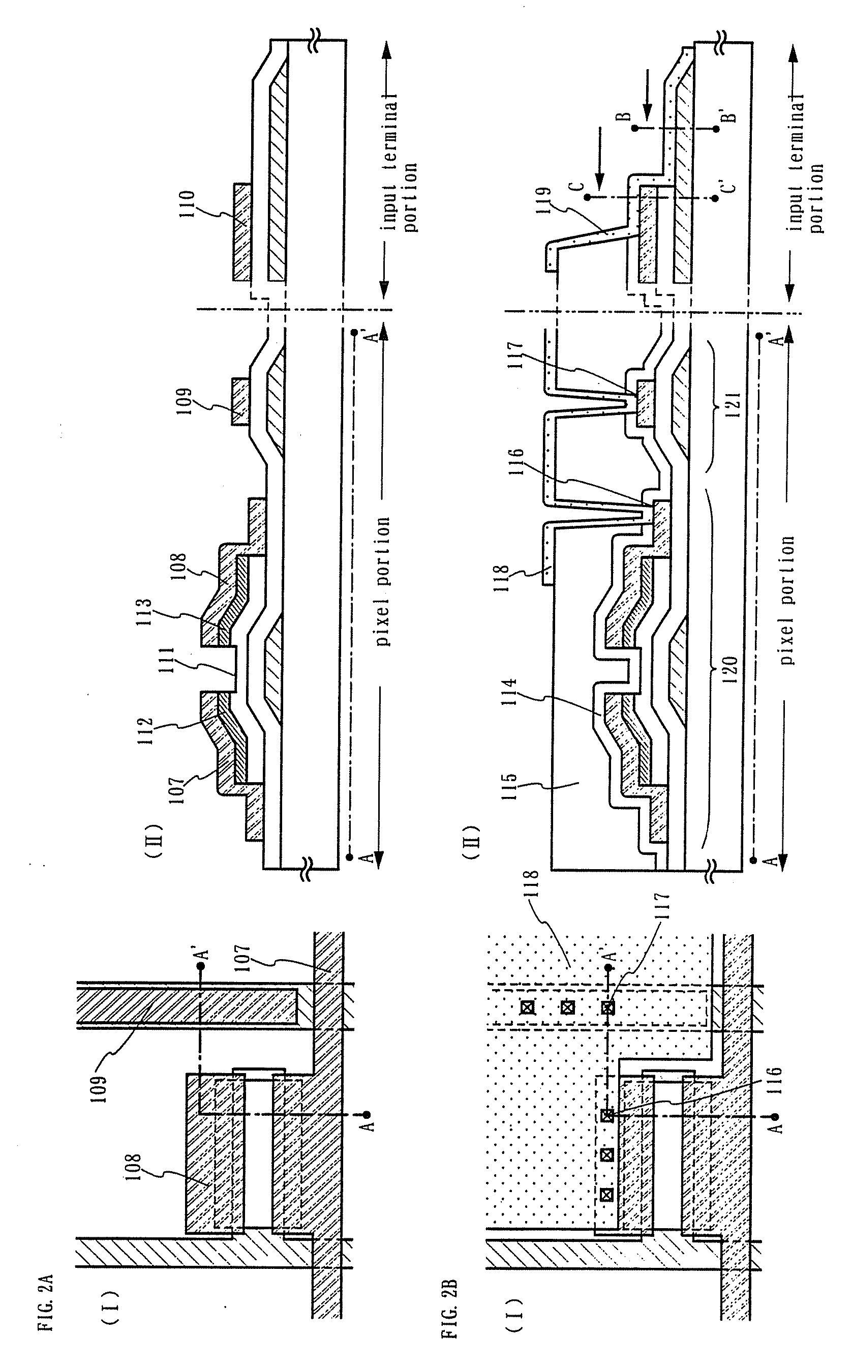
[0055]A first embodiment of the present invention will be described with reference to FIGS. 1A, 1B, 2A and 2B. This embodiment shows a method of manufacturing a liquid crystal display device, and a method of forming an inverse stagger type TFT of a pixel portion on a substrate and fabricating a storage capacitor connected to the TFT will be described in detail in the order of processes. Also, those figures show a process of fabricating an input terminal portion disposed on an end portion of the substrate for electric connection to a wiring of a circuit disposed on another substrate. In FIGS. 1A, 1B, 2A and 2B, portions (I) show top views whereas portions (II) show cross-sectional views taken along a line A-A′.

[0056]Referring to FIG. 1A, a substrate 101 may be made of a glass substrate such as barium boro-silicate glass or alumino boro-silicate glass which is represented by #7059 glass or #1737 glass made by Coming Inc. Alternatively, a stainless substrate or a ceramic substrate on w...

second embodiment

[0081]A description will be given of a method in which TFTs of the pixel portion are formed in the inverse stagger type on the substrate with a structure different from that in the first embodiment to manufacture the storage capacitor connected to the TFTs with reference to FIGS. 3A to 4B. Similarly, in FIGS. 3A, 3B and FIGS. 4A, 4B, their parts (I) are top views and cross-sectional views taken along a line A-A′ are shown by parts (II). The active matrix substrate manufactured by this embodiment corresponds to the transmission-type liquid crystal display device, and hereinafter differences from the first embodiment will be mainly described.

[0082]Referring to FIG. 3A, a substrate 201 may be made of a glass substrate such as barium boro-silicate glass or alumino boro-silicate glass which is represented by #7059 glass or #1737 glass made by Corning Inc. Alternatively, a stainless substrate or a ceramic substrate on which an oxide silicon film a nitride silicon film or the like is forme...

third embodiment

[0091]The second embodiment shows a method of manufacturing an active matrix substrate adaptive to the transmission type liquid crystal display device, and a third embodiment shows an example adaptive to a reflection type liquid crystal display device.

[0092]First, the processes shown in FIG. 3B are conducted in the same manner as that in the second embodiment. Then, as shown in the part (II) of FIG. 5, a third photolithography process is conducted to remove a part of the gate insulating film disposed on the terminal 204 by etching, to thereby form an aperture 230. Then, an electrically conductive layer is formed through the sputtering method and the vapor evaporation method as in the first embodiment, a resist mask pattern is formed through a fourth photolithography process, and a source wiring 231 and a drain wiring 232 are formed by etching as shown in FIG. 5. The drain wiring 32 serves as a pixel electrode and is so formed as to be overlapped with the storage capacitor wiring 203...


PUM

PropertyMeasurementUnit
temperatureaaaaaaaaaa
sizeaaaaaaaaaa
area resistanceaaaaaaaaaa

Abstract

In a semiconductor device, a first interlayer insulating layer made of an inorganic material and formed on inverse stagger type TFTs, a second interlayer insulating layer made of an organic material and formed on the first interlayer insulating layer, and a pixel electrode formed in contact with the second interlayer insulating layer are disposed on a substrate, and an input terminal portion that is electrically connected to a wiring of another substrate is provided on an end portion of the substrate. The input terminal portion includes a first layer made of the same material as that of the gate electrode and a second layer made of the same material as that of the pixel electrode. With this structure, the number of photomasks used in the photolithography method can be reduced to 5.

Description

BACKGROUND OF THE INVENTION[0001]1. Field of the Invention[0002]The present invention relates to a semiconductor device having a circuit structured by an inverse-stagger type or bottom gate type thin film transistor (hereinafter referred to as “TFT”) using a semiconductor film, and a method of manufacturing the semiconductor device. In particular, the present invention relates to a technique which is preferably applicable to an electro-optical device represented by a liquid crystal display device and an electronic device on which the electro-optical device is mounted. In the present invention, the semiconductor device is directed to all of devices that function using the semiconductor characteristics, and the electro-optical device and the electronic device on which the electro-optical device is mounted fall under the category of the semiconductor device.[0003]2. Description of the Related Art[0004]At present, in a note type personal computer (note personal computer) and a portable ...

Claims


Application Information

Patent Timeline
Patent Type & Authority Applications(United States)
IPC IPC(8): G02F1/136G02F1/1365G02F1/1368H01L29/786
CPCG02F1/1345G02F1/1368G02F2001/136231H01L27/1248G02F2001/136295H01L29/4908H01L27/1288G02F2001/13629G02F1/136231G02F1/13629G02F1/136295H01L29/511H01L29/78669
Inventor NAKAJIMA, SETSUOARAI, YASUYUKI
Owner SEMICON ENERGY LAB CO LTD
Why Eureka
Try Eureka