Nitride semiconductor device and method of manufacturing the same

a semiconductor and nitride technology, applied in semiconductor lasers, manufacturing tools, semiconductor laser structural details, etc., can solve the problems of defective appearance, chip shape cannot be stabilized, defective die bonding, etc., to achieve high energy density, reduce manufacturing costs, and reduce manufacturing costs

Active Publication Date: 2009-02-19
ROHM CO LTD
View PDF10 Cites 13 Cited by
  • Summary
  • Abstract
  • Description
  • Claims
  • Application Information

AI Technical Summary

Benefits of technology

[0024]The first region may be formed at the center in a laser beam scanning direction, and the second region may be formed on an end portion in the laser beam scanning direction. In this case, the depth of processing of the first region may be larger than the depth of processing of the second region. In the laser processing for forming the division guide groove, a laser beam having high energy density is applied to the substrate, so that multiphoton absorption can be caused on the substrate material. If the laser processing is performed up to edges of the substrate, the high-energy laser beam may be applied to a holder (adhesive sheet to which the substrate is bonded, for example) holding the substrate, and may lead to damage of the holder. In the laser processing for removing the debris, on the other hand, the laser beam is applied at relatively low energy density, and hence there is a little possibility that the holder is remarkably damaged by the laser beam. Therefore, the laser processing for forming the division guide groove is preferably performed in relation to only the first region at the center in the laser beam scanning direction, and the laser processing for removing the debris is preferably performed in relation to the overall region in the laser beam scanning direction. Thus, the holder is not damaged, and the debris can be reliably removed from the substrate. In this case, the second region provided on the end portion in the laser beam scanning direction is subjected to only the laser processing for removing the debris, to have a small depth of processing. In other words, the first region has a larger depth of processing than the second region.
[0025]When the group III nitride semiconductor layer forms a laser diode having a resonator, the laser trace may be formed parallelly to the resonator. If end faces of the resonator are formed by c-planes, for example, it is difficult to divide the substrate by cleavage in relation to the direction (a-plane or m-plane, for example) parallel to the laser resonator. Therefore, a deep division guide groove is formed by the laser processing utilizing multiphoton absorption, and the substrate is divided along this division guide groove. Deposits (debris adhering to a portion around the division guide groove) resulting from the formation of the division guide groove are removed from the surface of the substrate by the application of the laser beam having low energy density. Thus, a nitride semiconductor laser having high reliability with no defective appearance can be provided through the two-stage laser processing.

Problems solved by technology

If division guide grooves such as scribing lines are formed in a step of dividing the semiconductor substrate into individual chips, dividing positions deviate from the division guide grooves in a subsequent breaking step, and the chip shapes cannot be stabilized.
When the grooves are formed on the surface of the substrate, however, the substrate material is heated and scattered around as debris, to adhere to the surface of the substrate and contaminate the same.
This debris causes a defective appearance, defective die bonding, defective wire bonding, etc.

Method used


Image

  • Nitride semiconductor device and method of manufacturing the same
  • Nitride semiconductor device and method of manufacturing the same
  • Nitride semiconductor device and method of manufacturing the same

Examples


Embodiment Construction

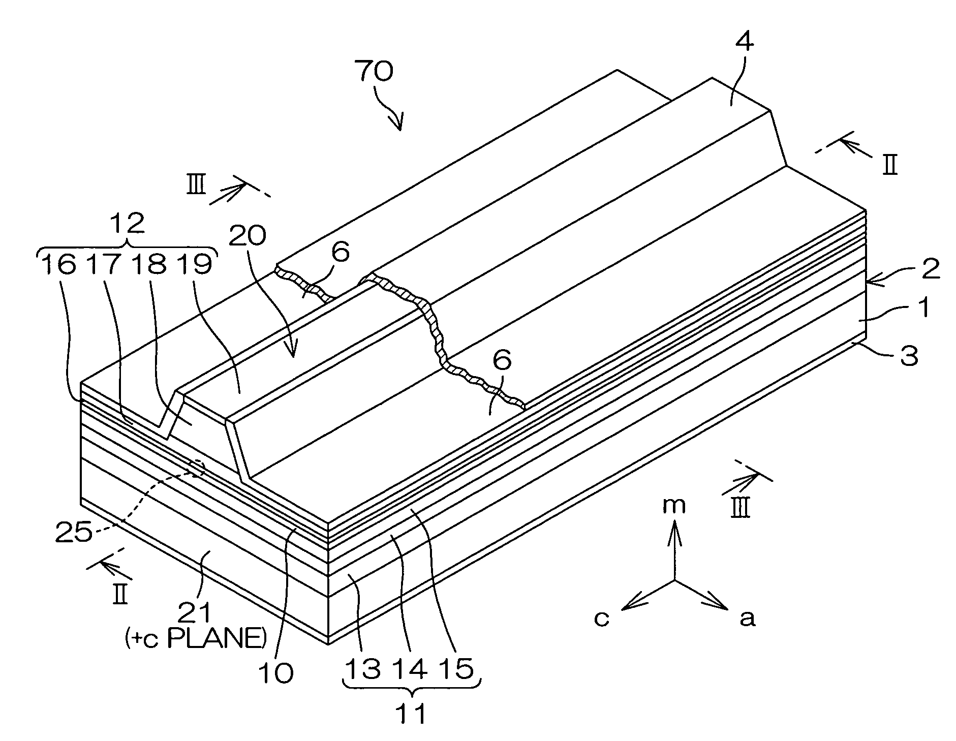
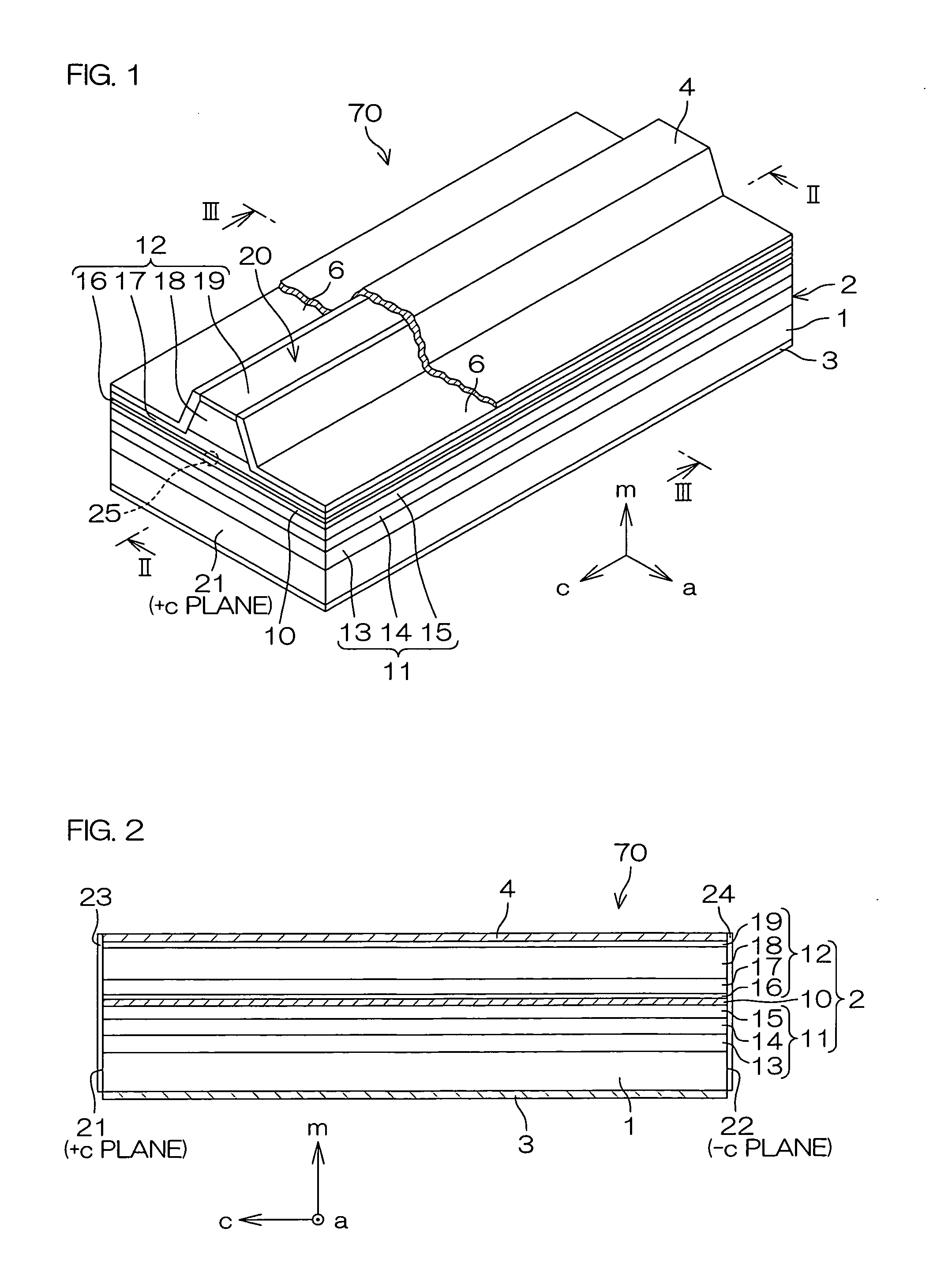
[0036]FIG. 1 is a perspective view for illustrating the structure of a semiconductor laser diode manufactured according to a method of manufacturing a nitride semiconductor device according to an embodiment of the present invention, FIG. 2 is a longitudinal sectional view taken along a line II-II in FIG. 1, and FIG. 3 is a cross sectional view taken along a line III-III in FIG. 1. Referring to FIGS. 1 to 3, arrows c, m and a denote the c-axis direction, the m-axis direction and the a-axis direction respectively.

[0037]This semiconductor laser diode 70 is a Fabry-Perot laser diode including a substrate 1, a group III nitride semiconductor multilayer structure 2 (group III nitride semiconductor layer) 2 formed on the substrate 1 by crystal growth, an n-side electrode 3 formed in contact with the back surface of the substrate 1 (surface opposite to the group III nitride semiconductor multilayer structure 2) and a p-side electrode 4 formed in contact with the surface of the group III nit...


PUM

PropertyMeasurementUnit
wavelengthaaaaaaaaaa
lengthaaaaaaaaaa

Abstract

A method of manufacturing a nitride semiconductor device includes the steps of: forming a division guide groove by applying a laser beam having a wavelength and energy density causing multiphoton absorption to a surface of a substrate having a group III nitride semiconductor layer grown on a major surface thereof; removing deposits from the surface of the substrate by applying a laser beam having the wavelength to the surface of the substrate at energy density causing substantially no multiphoton absorption on the substrate; and dividing the substrate along the division guide groove.

Description

BACKGROUND OF THE INVENTION[0001]1. Field of the Invention[0002]The present invention relates to a nitride semiconductor device having a structure obtained by forming group III nitride semiconductors on a substrate and a method of manufacturing the same. Group III nitride semiconductors are group III-V semiconductors employing nitrogen as a group V element, and typical examples thereof include aluminum nitride (AlN), gallium nitride (GaN) and indium nitride (InN), which can be generally expressed as AlxInyGa1-x-yN (0≦x≦1, 0≦y≦1 and 0≦x+y≦1).[0003]2. Description of Related Art[0004]A semiconductor light emitting device having a structure obtained by growing a group III nitride semiconductor layer on a GaN substrate is known in general. Typical examples thereof include a blue light emitting diode and a blue semiconductor laser. In addition to such light emitting devices, the group III nitride semiconductor is applied to transistors such as a power transistor and a high electron mobili...

Claims


Application Information

Patent Timeline
Patent Type & Authority Applications(United States)
IPC IPC(8): H01S5/323H01L33/00B23K26/00B23K26/16B23K26/364H01L21/301H01S5/02
CPCB82Y20/00H01L33/0095H01S5/34333H01S5/0202H01S5/22H01S5/0201
Inventor KOHDA, SHINICHI
Owner ROHM CO LTD
Why Eureka
Try Eureka