Graphene hybrid material and method for preparing same using chemical vapor deposition
a technology of chemical vapor deposition and hybrid materials, applied in the direction of polycrystalline material growth, crystal growth process, transportation and packaging, etc., can solve the problem of inability to synthesize graphen
- Summary
- Abstract
- Description
- Claims
- Application Information
AI Technical Summary
Problems solved by technology
Method used
Image
Examples
example 1
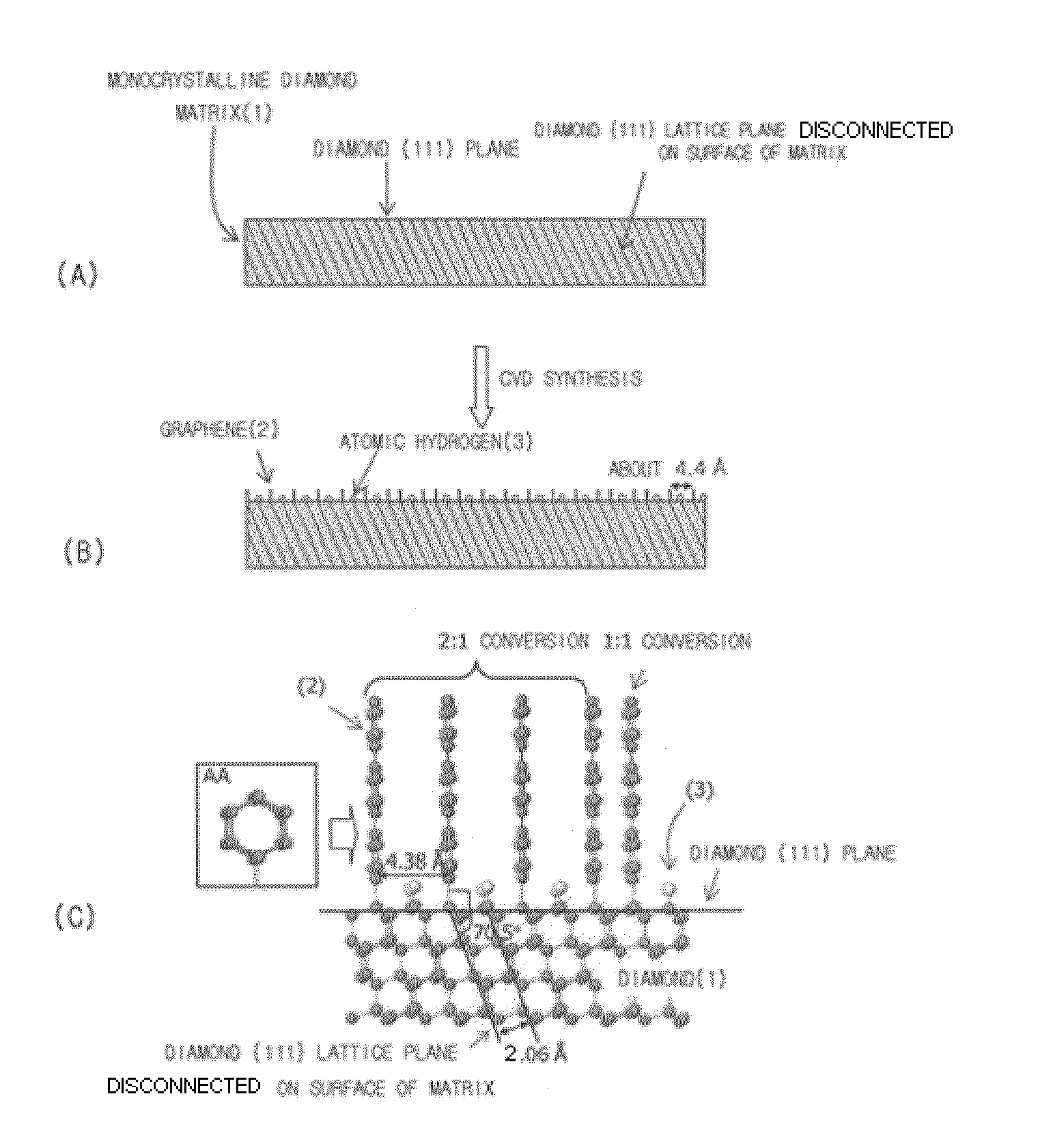
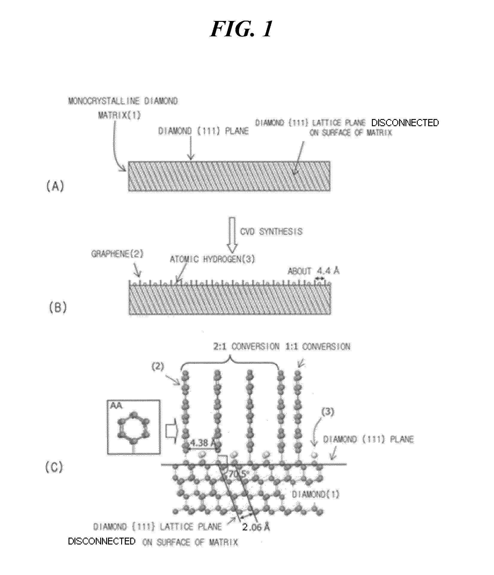
[0058]Graphene was synthesized using a method shown in FIG. 1. (110) monocrystalline diamond having {111} lattice planes disconnected on the surface thereof was used as a matrix. Direct-current plasma was used in CVD synthesis. 20% of methane (CH4) and 80% of hydrogen (H2) were used as reaction gases. The synthesis of graphene was conducted under the conditions of a pressure of 1 Torr, a gas flow rate of 200 sccm, a matrix temperature of about 70° C. and a synthesis time of 30 minutes.
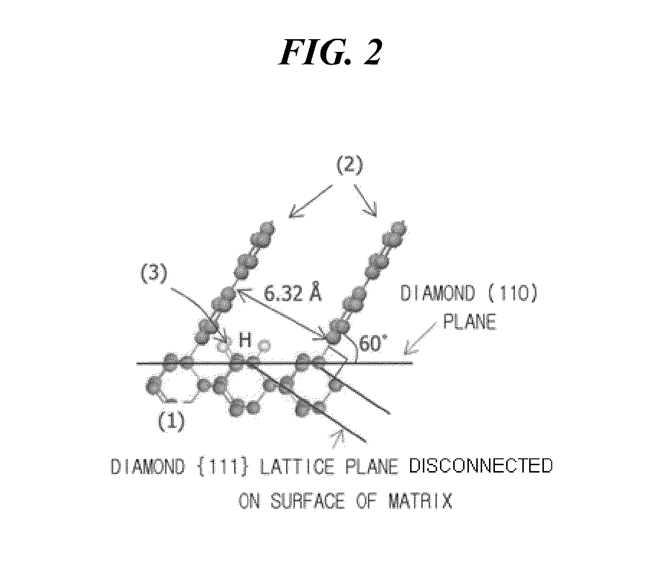
[0059]After the synthesis of graphene, a diamond matrix sample was collected and then observed by a high resolution transmission electron microscope (HRTEM). As a result, it was observed that the layers of graphene were vertically grown to a length of several nanometers (nm) while meeting with the surface of the matrix at an angle of 60°. When measured at a position spaced apart from the interface between diamond and graphene by 2 nm, the average interplanar spacing between the layers of graphene was 3...
example 2
[0060]Graphene was synthesized using a method shown in FIG. 3. First, a silicon substrate having a thickness of 1 mm was coated with a nanocrystalline diamond film using a direct-current plasma diamond synthesis apparatus. In this case, the coating of the silicon substrate was conducted under the conditions of a gas composition including 10% methane (CH4) and 90% hydrogen (H2), a pressure of 100 Torr, a gas flow rate of 200 sccm, a substrate temperature of about 70° C. and a synthesis time of 1 hour. The thickness of the nanocrystalline diamond film applied on the silicon substrate was 10 μm. As the results of Raman-analysis of the nanocrystalline diamond film, the nanocrystalline diamond film exhibited the properties of typical nanocrystalline diamond film.
[0061]Subsequently, an experiment for synthesizing graphene on the silicon substrate coated with the nanocrystalline diamond film was conducted. In this case, the synthesis of the graphene was conducted under the conditions of a ...
example 3
[0063]Graphene was synthesized using a method shown in FIG. 4. A nanocrystalline diamond film having a crystal grain size of 20˜30 nm, a thickness of 10 μm and a diameter of 4 inches formed on a silicon substrate having a thickness of 1 mm, which was formed using the same method as in Example 2, was used as a matrix.
[0064]Silica spheres having a size of about 10 μm were closely placed on the nanocrystalline diamond film and then the synthesis of graphene was performed using a multi-cathode direct-current plasma diamond synthesis apparatus. In this case, the synthesis of the graphene was conducted under the conditions of a gas composition including 10% methane (CH4) and 90% hydrogen (H2), a pressure of 100 Torr, a gas flow rate of 200 sccm, a silica sphere surface temperature of about 700° C. and a synthesis time of 30 minutes.
[0065]After the synthesis of graphene, a sample was collected and then analyzed using a high resolution transmission electron microscope (HRTEM). As a result, ...
PUM
| Property | Measurement | Unit |
|---|---|---|
| Temperature | aaaaa | aaaaa |
| Temperature | aaaaa | aaaaa |
| Pressure | aaaaa | aaaaa |
Abstract
Description
Claims
Application Information


