Solar cell

a solar cell and solar energy technology, applied in the field of solar cells, can solve the problems of inability to electrons and holes cannot contribute to power generation, and all photons less than the band gap of the semiconductor used to make the absorber of a solar cell are not capable of contributing to the power generation. , to achieve the effect of increasing the path length of ligh

Inactive Publication Date: 2009-02-26
THE RES FOUND OF STATE UNIV OF NEW YORK
View PDF9 Cites 27 Cited by
  • Summary
  • Abstract
  • Description
  • Claims
  • Application Information

AI Technical Summary

Benefits of technology

[0016]The present invention provides an apparatus and method to increase a path length of light by embedding small particles of spectral changing material in a matrix of high index (n>1) material on the face of a solar cell on which light is incident.

Problems solved by technology

Therefore, all photons less than the band gap of the semiconductor used to make the absorber of a solar cell are not capable of contributing to the power generation.
Conventional solar cell designs poorly convert UV photons to electrical energy since the high energy of these photons correlate to a large absorption coefficient.
Since electrons and holes need be separated and collected at the appropriate contact region in order to produce electrical power recombined electrons and holes cannot contribute to power generation.
Amorphous silicon-based solar cells have generated intense interest owing to low cost production and quick energy payback time.
However, these solar cells are known to degrade under sunlight via a process involving defect formation that reduces the amount of collected (power generating) hole-electron pairs through recombination.
Nonetheless, a significant amount of the above-band-gap light is typically not absorbed in the thinnest solar cell types, and all of the below-band-gap light is lost in all solar cell types.
These and other attempts to improve solar cell performance through the engineering of the semiconductor absorber layers increase the number of processing steps, raise the device complexity, and therefore increase the solar cell cost.
Furthermore, as multi-junction solar cell becomes more efficient at conversion of one particular solar spectrum (such as bight haze-less sunlight) it becomes less efficient under other conditions (for example overcast skies etc.).
However, it is typically absorbed in support structures and / or too near to the front surface of a solar cell to produce electric power.
Significantly more power is lost at longer wavelengths.

Method used


Image

  • Solar cell
  • Solar cell
  • Solar cell

Examples


Embodiment Construction

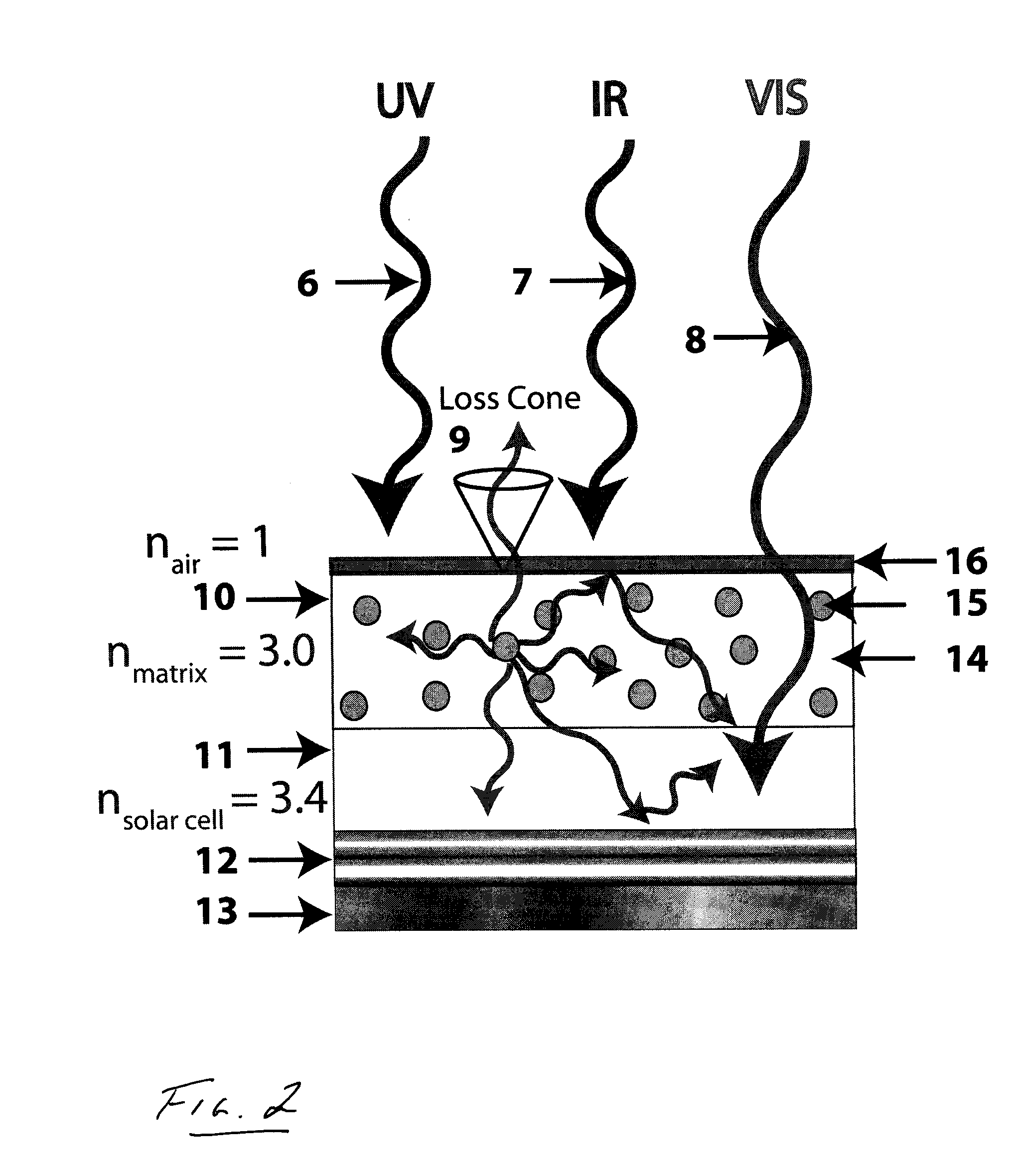
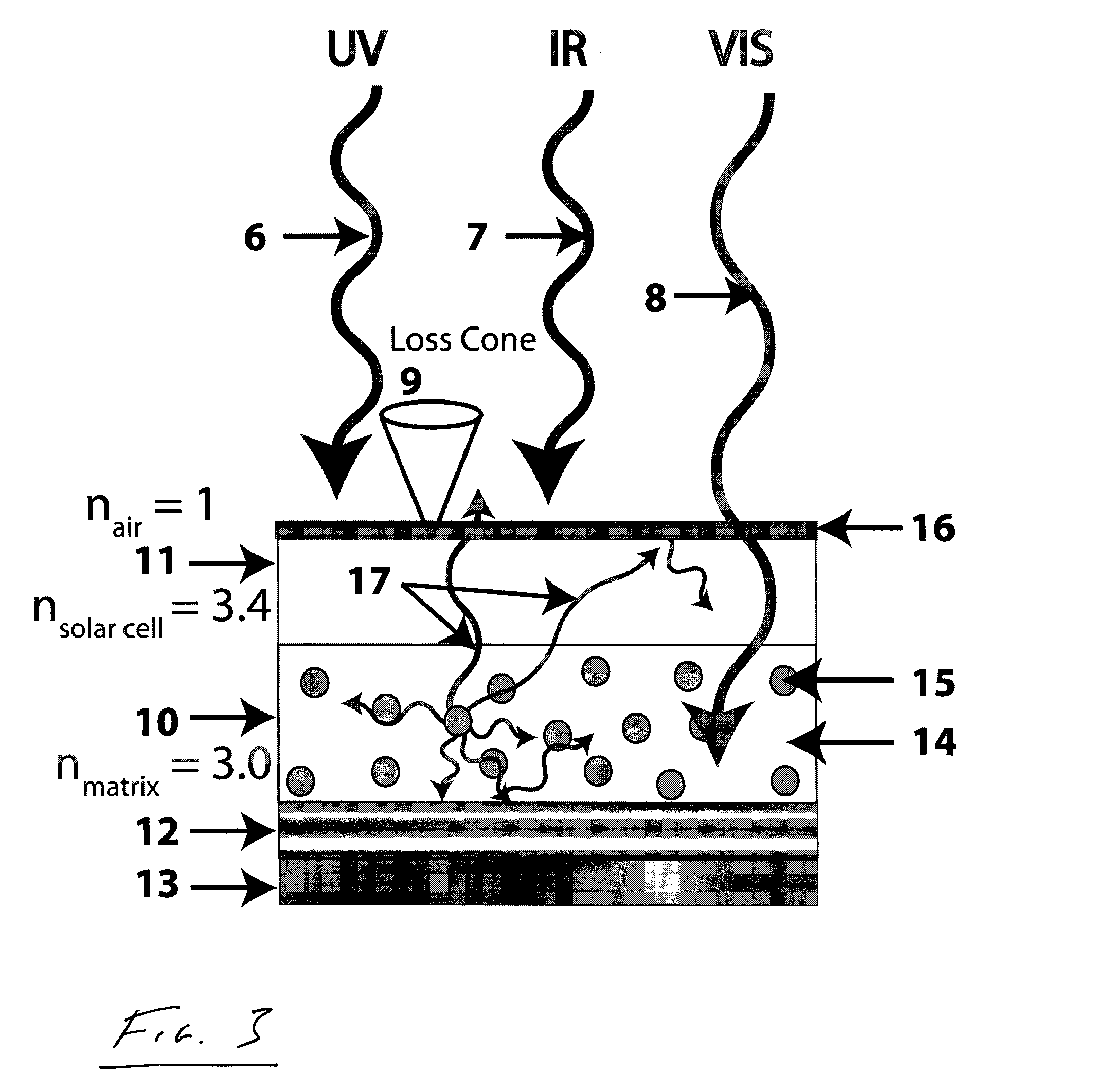
[0022]The following detailed description of preferred embodiments of the invention is provided with reference to the accompanying drawings. In describing the invention, explanation about related functions or constructions known in the art are omitted for the sake of clearness in understanding the concept of the invention, to avoid obscuring the invention with unnecessary detail.

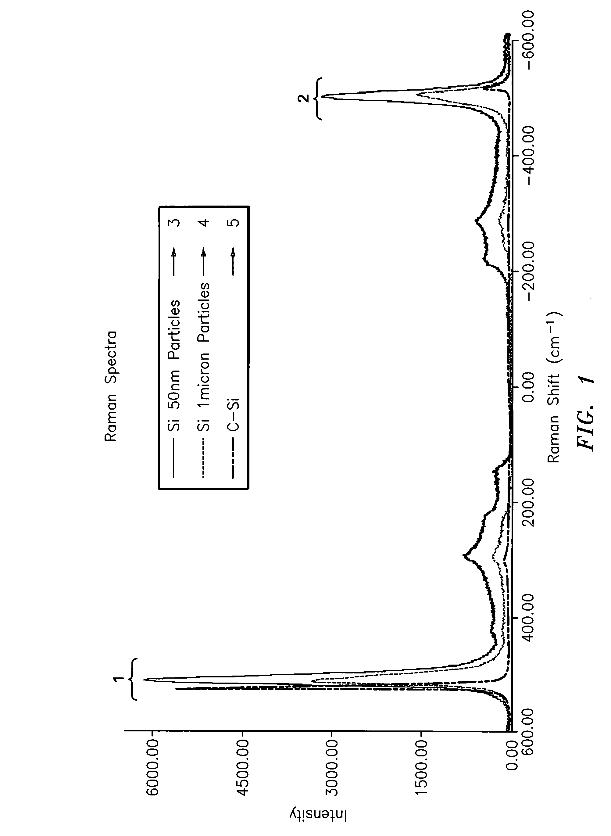
[0023]The present invention exploits specific material properties to change the wavelength of light through an interaction involving the vibration of atoms known as Raman scattering. Raman scattering in silicon and silicon particles is particularly large.

[0024]Raman scattering can both increase and decrease photon energy a portion of an incident photon beam will be up-converted in energy. In turn these up-converted photons are useable by the solar cell component.

[0025]As shown in FIG. 1, Raman scattering is characterized by the interaction of light with quantized atomic vibrations within a material known as p...


PUM


Abstract

Disclosed is a photovoltaic solar cell and method for producing same for conversion of light into electric power using a composite film having micron sized down to nanometer sized particles sufficiently sized for precise light scattering. A matrix material is further provided having a substantially different refractive index to provide a refractive index contrast for light scattering.

Description

PRIORITY[0001]This application claims priority to U.S. Provisional Application No. 60 / 950,234, filed Jul. 17, 2007, to U.S. Provisional Application No. 61 / 081,492, filed Jul. 17, 2008, and to U.S. Provisional Application No. 61 / 081,494, filed Jul. 17, 2008, the contents of each of which are incorporated herein by reference.BACKGROUND OF THE INVENTION[0002]The present invention relates to an apparatus and method for spectral modification to improve solar cell efficiency.[0003]Photovoltaic solar cells convert light to energy via the well-known process of photo-induced electron transition from valance to conduction bands when the photon energy exceeds the energy needed by the photon to transition from the valence band to the conduction band. Fundamental quantum mechanics largely precludes the possibility of an electron being excited from the valance to the conduction band unless the photon energy is equal to or greater than the valance band to conduction band energy (known as the band ...

Claims


Application Information

Patent Timeline
Patent Type & Authority Applications(United States)
IPC IPC(8): H01L31/055H01L31/04
CPCH01L31/055H01L31/0547Y02E10/52
Inventor FORTMANN, CHARLES M.
Owner THE RES FOUND OF STATE UNIV OF NEW YORK
Why Eureka
Try Eureka