Image sensor and electromagnetic radiation imaging device

a technology of electromagnetic radiation imaging and image sensor, applied in the field of image, can solve the problems of unstable circuit operation, phase bias points cannot maximize the signal-to-noise ratio (s/n ratio) of an image to be obtained by an electric field modulation system, and the thz electromagnetic radiation imaging device becomes complex, so as to avoid unstable state, ensure stable circuit operation, and achieve high-speed thz electromagnetic radiation imaging

Active Publication Date: 2009-03-05
PANASONIC CORP
View PDF11 Cites 52 Cited by
  • Summary
  • Abstract
  • Description
  • Claims
  • Application Information

AI Technical Summary

Benefits of technology

[0057]With this structure, it becomes possible to avoid an unstable state caused when the fifth capacitor and the fourth capacitors are simultaneously connected to the second capacitor or the third capacitor, that is, the gate of the first transistor or the second transistor, and the stable operation of the circuit is ensured.
[0058]With the image sensor according to the present invention, it is possible to output the difference between the signals of the different photodiodes within a period for accumulating signal for one frame image. In particular, when polarized light filters each of which has a different polarization property and each of which is arranged above each of the photodiodes included in the pair of photodiodes, it becomes possible to output the d

Problems solved by technology

The following problems, however, arise with the above-mentioned techniques.
Concerning the object moving and performing in a short time equal to or less than image acquisition time, however, image distortion, out-of-focus image and the like occur, and a good image cannot be obtained.
In this case, however, these phase bias points cannot maximize a signal-to-noise ratio (S/N ratio) of an image to be obtained by an

Method used


Image

  • Image sensor and electromagnetic radiation imaging device
  • Image sensor and electromagnetic radiation imaging device
  • Image sensor and electromagnetic radiation imaging device

Examples


embodiment 1

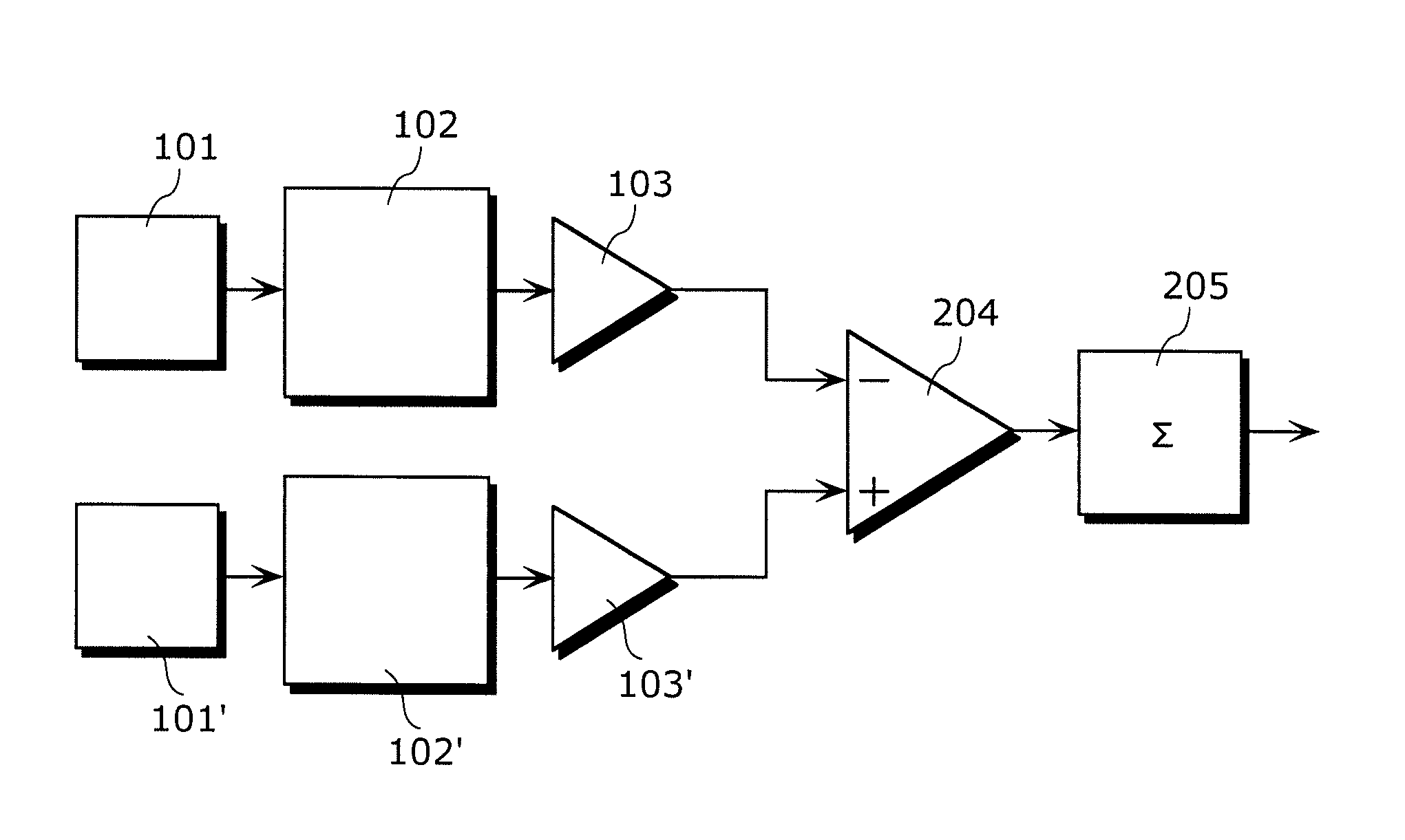
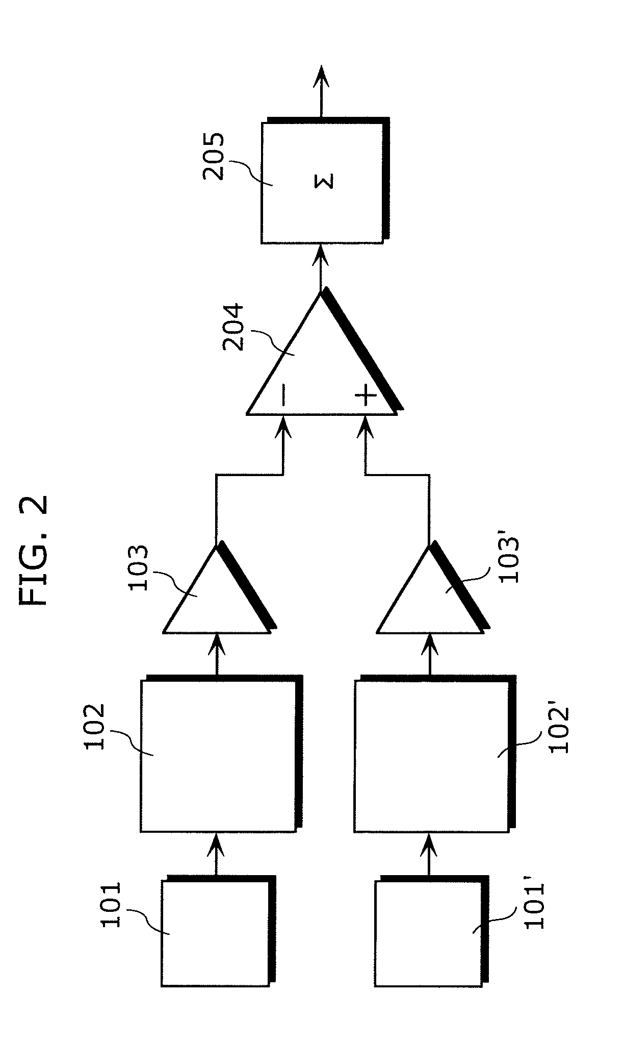
[0078]The following describes an image sensor according to an embodiment 1 of the present invention with reference to FIGS. 2 to 6.

[0079]FIG. 2 is a circuit diagram illustrating an operating principle of the image sensor according to the embodiment 1.

[0080]The circuit includes a pair of adjacent photodiodes 101 and 101′, a pair of readout circuits 102 and 102′, a pair of signal output circuits 103 and 103′, a difference circuit 204, and an integration circuit 205. In the circuit, the respective readout circuits 102 and 102′ transfer signal charges accumulated by the photodiodes 101 and 101′ to the signal output circuits 103 and 103′ in a subsequent stage. Further, a signal output from each of the photodiodes 101 and 101′ is inputted to the difference circuit 204 in a subsequent stage, and, for example, a signal showing a difference between different polarization components or different wavelength components (difference signal) is detected. Since a difference output is extremely weak...

embodiment 2

[0099]The following describes an image sensor according to an embodiment 2 of the present invention with reference to FIGS. 7 to 10.

[0100]FIG. 7 illustrates a detailed circuit configuration in a pixel of the image sensor according to the embodiment 2. It is to be noted that FIG. 7 illustrates a circuit configuration in a pixel including the photodiodes 302 and 302′ of FIG. 3.

[0101]Also in the image sensor according to the embodiment 2, a polarized light filter is arranged for each pair of photodiodes in the same manner as in the image sensor of FIG. 3, and the signal process driving circuit 304, the row scanning circuit 305, and the column scanning circuit 306 are arranged around a pixel region where the plural pixels are arranged two-dimensionally as shown in FIG. 4. In contrast, what differs from the image sensor according to the embodiment 1 are a readout circuit which reads signals of the pair of photodiodes in the pixel, a difference circuit which calculates a difference, and a...

embodiment 3

[0123]The following describes an image sensor according to an embodiment 3 of the present invention with reference to FIGS. 11 and 12.

[0124]FIG. 11 illustrates a detailed circuit configuration in a pixel of the image sensor according to the embodiment 3. It is to be noted that FIG. 11 illustrates a circuit configuration in the pixel including the photodiodes 302 and 302′ of FIG. 3.

[0125]Also in the image sensor according to the embodiment 3, a polarized light filter is arranged for each pair of photodiodes in the same manner as in the image sensor of FIG. 3, and the signal process driving circuit 304, the row scanning circuit 305, and the column scanning circuit 306 are arranged around a pixel region where the plural pixels are arranged two-dimensionally as shown in FIG. 4. In addition, a configuration of a readout circuit which reads a signal of the pair of photodiodes in the pixel is the same as in the image sensor according to the embodiment 2, and further a difference circuit ob...


PUM


Abstract

To provide a small-size image sensor and electromagnetic radiation imaging device which can obtain a good image without relying on the condition of an object, the image sensor including a plurality of pixel units arranged two-dimensionally, wherein each of the plurality of pixel units includes: a first photodiode and a second photodiode; a readout circuit which reads a signal generated by the first photodiode and a signal generated by the second photodiode, and outputs the read signals, the readout circuit being connected to the first photodiode and the second photodiode; and a difference circuit which outputs a difference signal corresponding to a difference between the signal read from the first photodiode and the signal read from the second photodiode, the difference circuit being connected to the readout circuit.

Description

BACKGROUND OF THE INVENTION[0001](1) Field of the Invention[0002]The present invention relates to image sensors and devices to which the image sensor is applied and, in particular, to an image sensor and an electromagnetic radiation imaging device which image THz electromagnetic radiation.[0003](2) Description of the Prior Art[0004]In recent years, the development of THz electromagnetic radiation imaging devices has been advanced for security check, a medical test, a food analysis, a drug analysis, environmental monitoring, and so on (See the following: Non-patent Reference 1: Kiyomi Sakai ed., “Terahertz Optoelectronics”, Springer Verlag, 2005, pp. 331-381; Non-patent Reference 2: B. B. Hu and M. C. Nuss, Opt. Lett. Vol. 20, p. 1716, (1995); Patent Reference 1: Japanese Unexamined Patent Application Publication No. 2002-5828; Patent Reference 2: Japanese Unexamined Patent Application Publication No. 2004-20504; and Patent Reference 3: Japanese Unexamined Patent Application Publicat...

Claims


Application Information

Patent Timeline
IPC IPC(8): H01L27/00G01J1/20G01N21/35G01N21/3586G01S13/89H01L27/146H04N5/335H04N5/357H04N5/369H04N5/374
CPCG01J1/04G01J1/0429G01J1/1626H01L27/14641G01J1/46G01N21/3581G01J1/4228
Inventor HIROSE, YUTAKA
Owner PANASONIC CORP
Why Eureka
Try Eureka