Semiconductor device

a technology of semiconductor devices and semiconductor layers, applied in semiconductor devices, diodes, electrical apparatus, etc., can solve the problems of difficult manufacturing of passive elements on this layer using conventional processes, and the inability of conventional processes to use such integration of passive elements, and achieves low power consumption, high performance, and high q value.

Inactive Publication Date: 2009-03-05
RENESAS TECH CORP
View PDF4 Cites 169 Cited by
  • Summary
  • Abstract
  • Description
  • Claims
  • Application Information

AI Technical Summary

Benefits of technology

[0052]Also, by applying back bias voltage in a positive direction, a passive element with small parasitic capacitance and a high Q value can be provided.
[0053]Accordingly, since a high-quality analog circuit and a high-frequency circuit are

Problems solved by technology

When the passive elements are intended to be further integrated on the chip equipped with the above-mentioned FDSOI devices, since a substrate different from a conventional bulk device is used, a conventional process cannot be used for such integration o

Method used


Image

  • Semiconductor device
  • Semiconductor device
  • Semiconductor device

Examples


embodiment 1

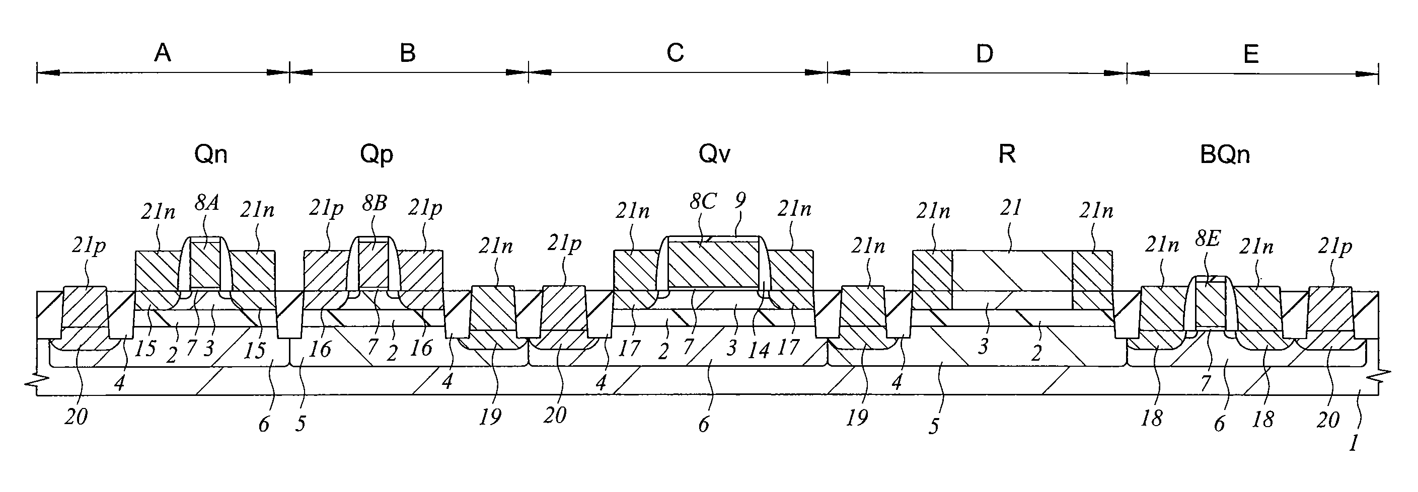
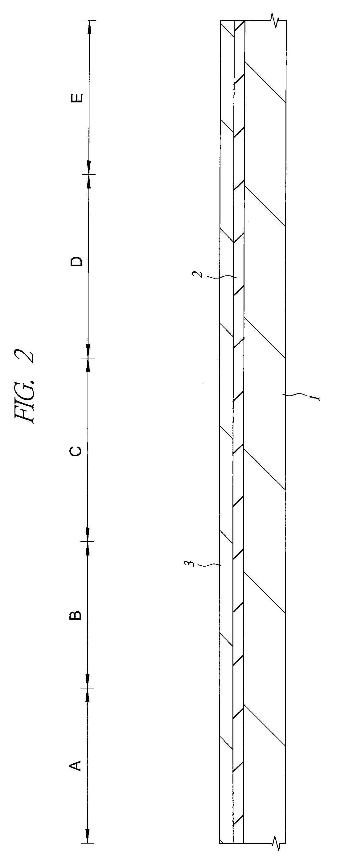
[0079]A manufacturing method for a semiconductor device according to the present invention will be described in order of steps with reference to FIGS. 2 to 11. Regions shown by the reference numerals “A” to “D” in each Figure are FDSOI device forming regions. Among them, a region (A) represents a NMOS transistor forming region; a region (B) a PMOS transistor forming region; a region (C) a MOS varactor forming region; and a region (D) a resistor forming region. Also, a region (E) represents a bulk device forming region, but, for simplifying its explanation, only a bulk NMOS transistor will be illustrated and described and illustration and description of other devices will be omitted.

[0080]First, as shown in FIG. 2, an SOI substrate comprising a supporting substrate 1, a BOX layer 2, and an SOI layer 3 is provided. The supporting substrate 1 is formed of a p type monocrystalline silicon having a plane orientation (100) and a resistivity of approximately 5 Ωcm. The SOI layer 3 is forme...

embodiment 2

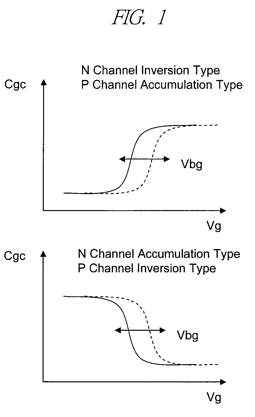
[0101]In the present embodiment, electrical characteristics of the MOS varactor Qv manufactured according to Embodiment 1 will be described. This MOS varactor is configured as an N channel inversion type of a combination shown in above Table 1. That is, the p type well 6 is doped with p type impurity (boron) of order of 1017 / cm3 while the impurity concentration of the SOI layer 3 is suppressed by order of 1016 / cm3. The n+ type semiconductor region (source and drain) 17 is doped with n type impurity (for example, arsenic) of approximately 1020 / cm3, and the portion (p+ type semiconductor region 20) contacting with the supporting substrate 1 (p type well 6) is doped with p type impurity (boron) of approximately 1020 / cm3. The thickness of the gate dielectric 7 is 2 nm, and that of the BOX layer 2 is 10 nm. Also, the film thickness of the SOI layer 3 after formation of the device is 15 nm.

[0102]The capacitance characteristic of the MOS varactor Qv formed under the above condition is show...

embodiment 3

[0108]In the present embodiment, there will be described a device layout in the case where the MOS varactor Qv formed in above Embodiment 1 is a differential type, and described a voltage controlled oscillation circuit using this differential type MOS varactor Qv.

[0109]First, FIG. 16 shows a voltage controlled oscillation circuit (VCO) in which the type MOS varactor Qv is a differential type. This voltage controlled oscillation circuit comprises two NMOS transistors Qn, two MOS varactors Qv, and two inductors (C). The NMOS transistors Qn and the MOS varactors Qv are ones formed in above Embodiment 1. A condition of manufacturing the device is the same as that of above Embodiment 2. In order to operate the FDSOI device under this condition, power voltage Vdd is set at 1.2 V. At this voltage, the NMOS transistors Qn and the MOS varactors Qv were successfully operated without any problems.

[0110]In the voltage controlled oscillation circuit shown in FIG. 16, two NMOS transistors Qn and ...


PUM


Abstract

A semiconductor device having a passive element whose characteristic is adjustable even after manufacture by applying back bias voltage is provided. Formed on a main surface of a SOI substrate comprising a supporting substrate, a BOX layer, and an SOI layer is a MOS varactor comprising a gate dielectric formed on a surface of the SOI layer, a gate electrode formed on the gate dielectric, and a n+ type semiconductor region formed in the SOI layer located on both sides of the gate electrode. The MOS varactor, is configured so that capacitance formed by the SOI layer, gate dielectric, and gate electrode is varied by applying bias voltage to the supporting substrate (p type well) under the gate electrode.

Description

CROSS-REFERENCE TO RELATED APPLICATION[0001]The present application claims priority from Japanese patent application No. JP 2007-229811 filed on Sep. 5, 2007, the content of which is hereby incorporated by reference into this application.TECHNICAL FIELD OF THE INVENTION[0002]The present invention relates to a semiconductor device, particularly, the present invention relates to a technique that is effectively applied to a semiconductor device comprising a varactor (variable-capacitance device) or a resistor used in a wireless information communication apparatus and the like.BACKGROUND OF THE INVENTION[0003]A silicon field effect semiconductor device for logic element has continuously improved its performance such as integration and operating speed and reduced power consumption per device by miniaturizing strenuously the semiconductor device. However, since generation in which a processing dimension of the device is less than 50 nm comes, it has become difficult to achieve both of imp...

Claims


Application Information

Patent Timeline
IPC IPC(8): H01L29/788H01L29/06
CPCH01L21/82385H01L21/823878H01L21/84H01L27/0207H01L27/1203H01L29/93H01L27/0629H01L27/1207
Inventor SUGLL, NOBUYUKITSUCHIYA, RYUTAKIMURA, SHINICHIRO
Owner RENESAS TECH CORP
Why Eureka
Try Eureka