Wafer Level Chip Size Package For MEMS Devices And Method For Fabricating The Same

Active Publication Date: 2009-03-05
CHINA WAFER LEVEL CSP
View PDF9 Cites 21 Cited by
  • Summary
  • Abstract
  • Description
  • Claims
  • Application Information

AI Technical Summary

Benefits of technology

[0012]The present invention intends to solve the problems existing in prior art WLCSP, and to provide an

Problems solved by technology

However, both of them are ordinarily very expensive, for many conventionally produced MEMS components, the processes of packaging may take up about 70-85% from the total fabrication cost.
Moreover, the packages in most cases are not small enough for handhold applications like cell phones.
Although the Shellcase technique is quite suitable for optical and image sensors, e.g., charge-coupled devices (CCD) and/or CMOS imagers integrated on a silicon wafer, it is actually not fully satisfiable for MEMS devices.
First, in most cases, MEMS package has to provide inert gas filling in or high vacuum so as to protect the fragile movable parts, which requires high hermetic packaging, but the epoxy made cav

Method used


Image

  • Wafer Level Chip Size Package For MEMS Devices And Method For Fabricating The Same
  • Wafer Level Chip Size Package For MEMS Devices And Method For Fabricating The Same
  • Wafer Level Chip Size Package For MEMS Devices And Method For Fabricating The Same

Examples


embodiment 1

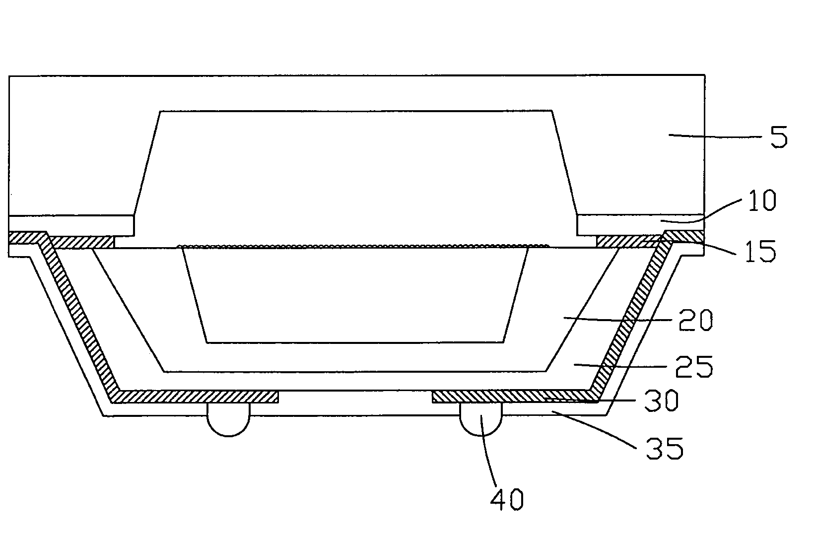
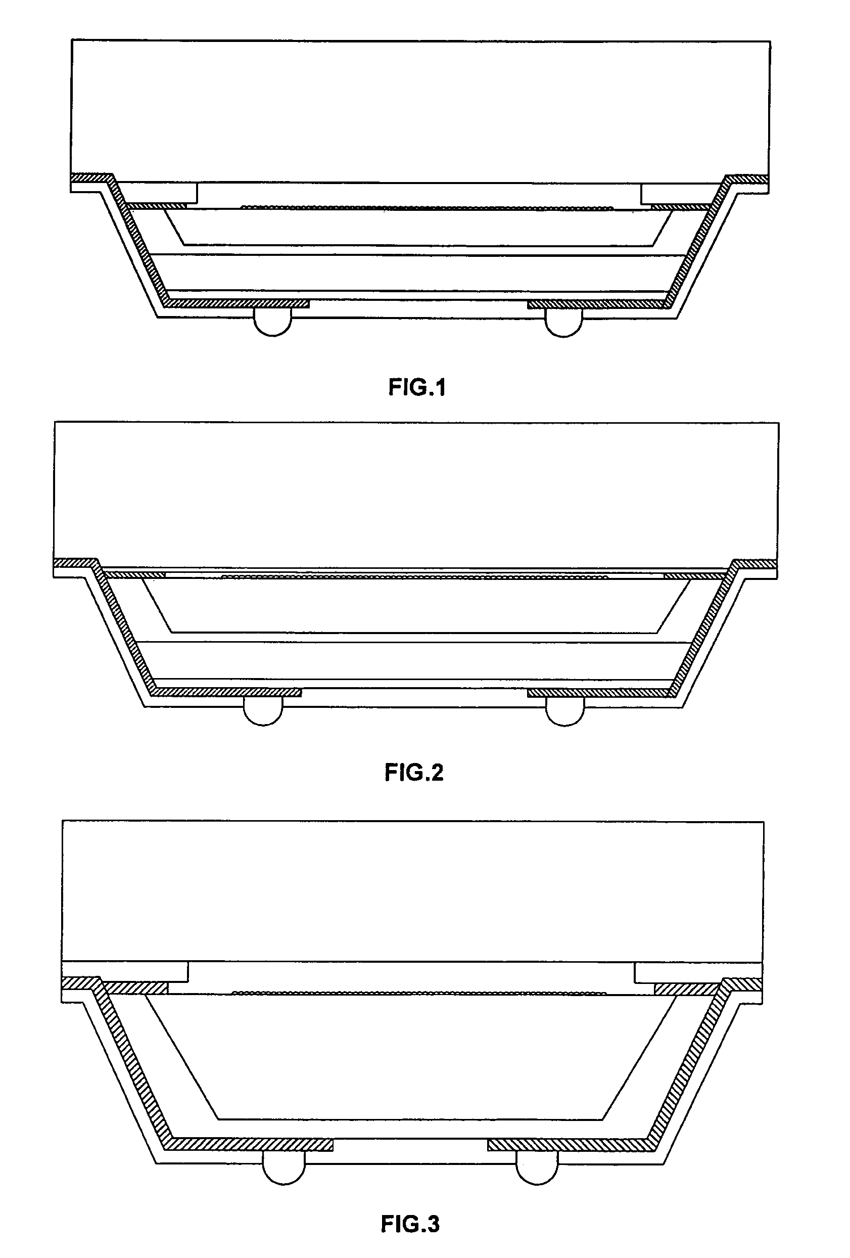
[0067]As shown in FIG. 14, according to embodiment 1 of the present invention, a wafer level chip size package for MEMS devices includes a substrate wafer 20, a cap substrate 5, a cushion layer 25, a layer of redistribution leads 30, solder mask 35 and a plurality of solder bumps 40.

[0068]The substrate wafer 20 has formed thereon MEMS dies formed with certain MEMS structures, such as gears, hinges, slides, etc. There are also electrical terminals, preferably in the form of so called compatible pads 15 disposed at the periphery of each of the MEMS dies on the substrate wafer 20.

[0069]The cap substrate 5 has cavities which can be filled in inert gas with a certain pressure. The cap substrate 5 includes cavity walls 10 by which the cap substrate 5 is combined with the substrate wafer 20, each of the MEMS dies being encased within a corresponding cavity. Preferably though not necessarily, the depth of cavities is within the approximate range of 300-400 um, the thickness of cavity walls ...

embodiment 2

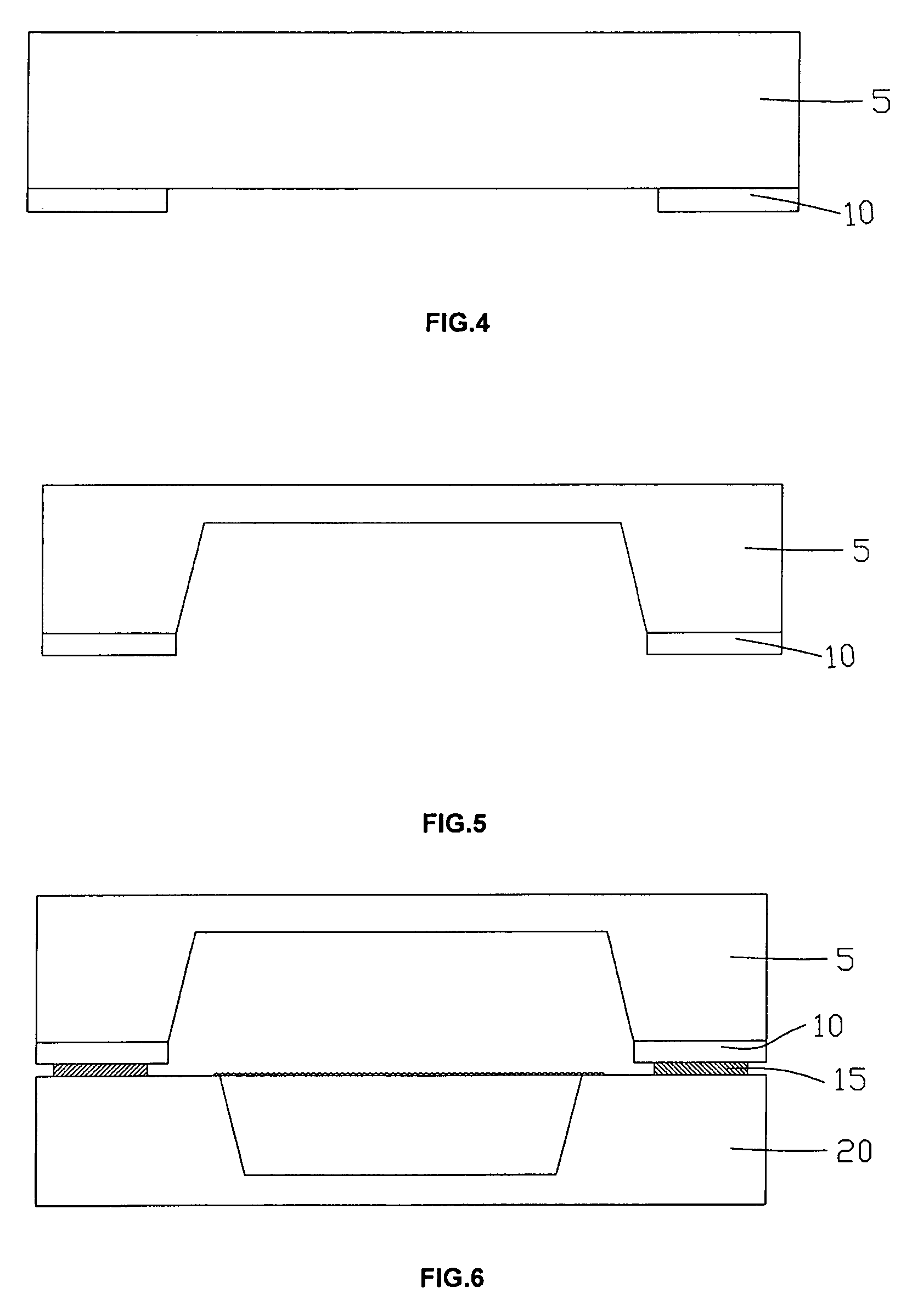
[0089]According to embodiment 2 of the present invention, instead of the steps illustrated in FIG. 4 and FIG. 5, an alternative method of forming the cavity walls 10 is illustrated from FIG. 15 to FIG. 18.

[0090]As illustrated in FIG. 15, deposit a passivation layer 45 on the front side of the cap substrate 5 by PECVD (plasma enhanced chemical vapor deposition), spin coat photo resist 50 on the passivation layer 45, make pattern by lithography, the area which need not to be etched should be covered by photo resist 50.

[0091]As illustrated in FIG. 16, plasma etch at the front side of the cap substrate, the photo resist 50 will protect the passivation layer 45 from being etched while the exposed passivation layer 45 will be etched. After etching, strip the photo resist 50, the pattern of the passivation layer 45 is the same as that of the photo resist 50.

[0092]As illustrated in FIG. 17, make cavities on the cap substrate 5 by wet etching or dry etching, utilize the passivation layer 45 ...


PUM


Abstract

The present invention provides a wafer level chip size package having cavities within which micro-machined parts are free to move, allowing access to electrical contacts, and optimized for device performance. Also a method for fabricating a wafer level chip size package for MEMS devices is disclosed. This packaging method provides a well packed device with the size much closely to the original one, making it possible to package the whole wafer at the same time and therefore, saves the cost and cycle time.

Description

CROSS-REFERENCE TO RELATED APPLICATIONS[0001]The present invention claims priority from Chinese Patent Application Ser. No. 200710131491.3 filed Aug. 31, 2007, entitled “Wafer Level Chip Size Package For MEMS Devices And Method For Fabricating The Same” by Wang et al., which is incorporated herein by reference for all purposes.FIELD OF THE INVENTION[0002]The present invention relates generally to wafer level chip size package, and more particularly to wafer level chip size package for micro-electromechanical system (MEMS) devices and methods for fabricating the same.BACKGROUND OF THE INVENTION[0003]With the miniaturization of electronic devices and increase of circuit density in semiconductor industry, technology of chip size package (CSP) is now under great development, of which the package size is similar to the semiconductor chip encased therein. The ratio of a typical CSP to the edge dimension is no larger than 120% as defined by Joint Electron Device Engineering Council (JEDEC)...

Claims


Application Information

Patent Timeline
IPC IPC(8): H01L23/04H01L21/50
CPCB81B2207/097B81C1/00301B81C2203/0118H01L23/10H01L2924/0002H01L23/3114H01L2924/00
Inventor WANG, ZHIQIYU, GUOQINGXU, QINQINWANG, WEI
Owner CHINA WAFER LEVEL CSP
Why Eureka
Try Eureka