
Interconnect structures with patternable low-k dielectrics and method of fabricating same

a technology of low-k dielectrics and interconnect structures, which is applied in the direction of electrical equipment, semiconductor devices, semiconductor/solid-state device details, etc., can solve the problems of difficult implementation of low-k materials such as silicon oxide, and the fundamental weaker electrical and mechanical properties of low-k dielectrics compared to silicon oxide, so as to reduce the complexity of the fabrication of current interconnect structures, reduce the number of layers, and reduce the time and cost of fabrication

Inactive Publication Date: 2009-03-26
GLOBALFOUNDRIES INC
View PDF79 Cites 57 Cited by
  • Summary
  • Abstract
  • Description
  • Claims
  • Application Information

AI Technical Summary

Benefits of technology

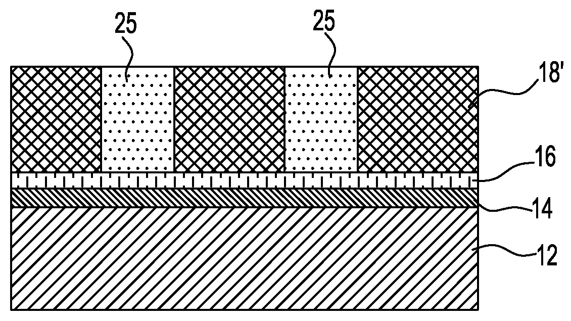
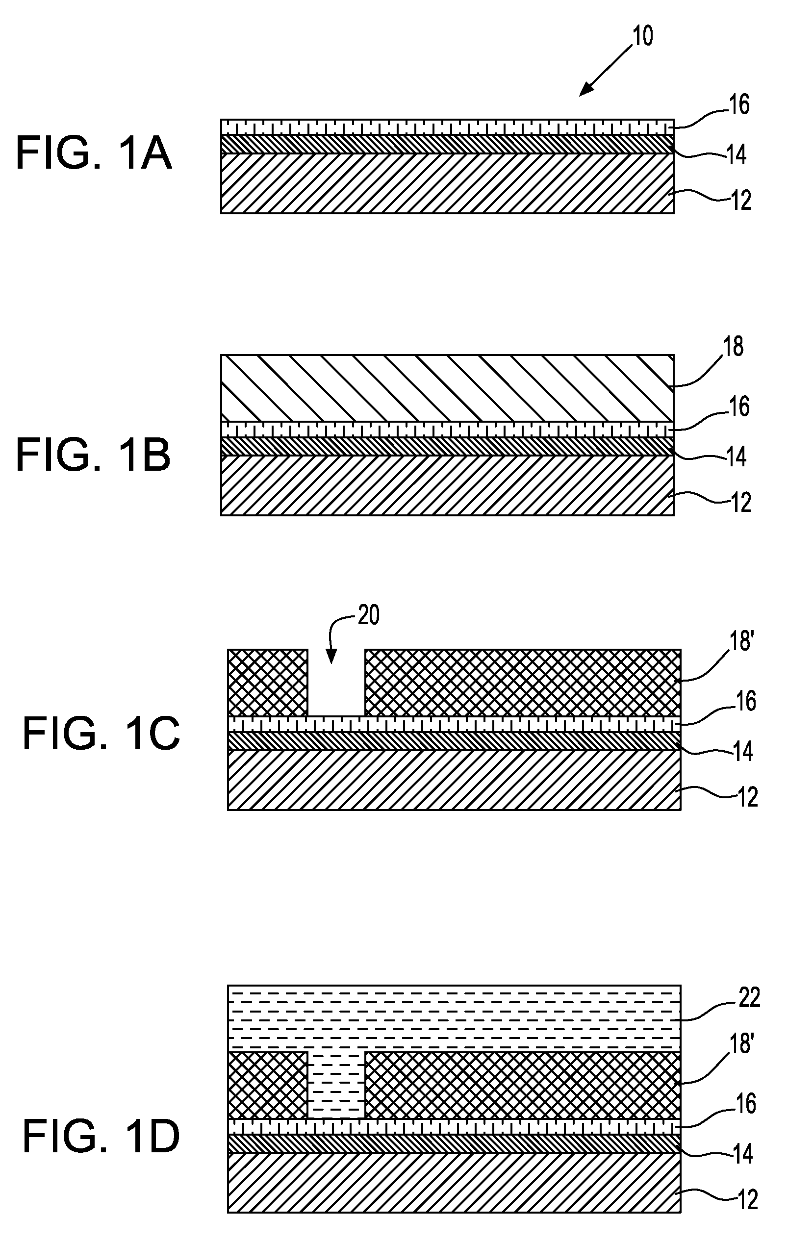
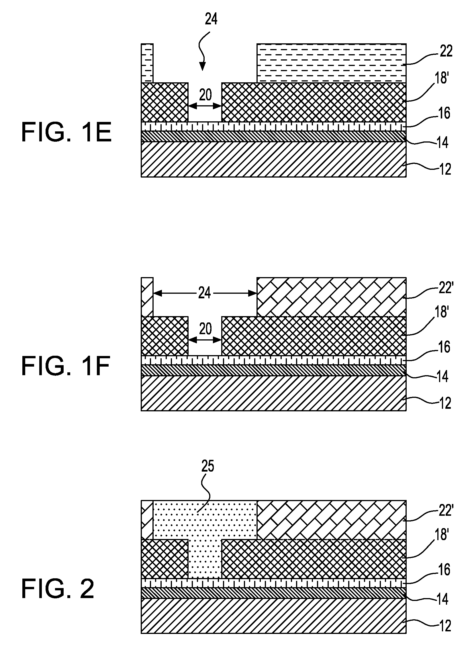
[0021]This invention circumvents the prior art drawbacks of current integration by combining the functions of a photoresist and a dielectric material into one material. This one material, called a photo-patternable low-k dielectric (or patternable low-k material for short), acts as a photoresist during the lithographic patterning process, and as such, no separate photoresist is required. After lithographic patterning, the patternable low-k dielectric is subsequently converted into a low-k material during a post patterning cure. In this way, the inventive method avoids plasma etching and the complex sacrificial film stack and processes required for conventional patterning.
[0050]This patternable low-k method of the present invention dramatically reduces the complexity in the fabrication of current interconnect structures. The photoresist used in the prior art integration is no longer needed. In addition the present invention also does not utilize a plasma etching step for patterning as also required in the prior art interconnect processing schemes. It is further noted that the inventive method reduces the number of layers required to fabricate the interconnect structure and, as such, the present invention reduces the time and cost of fabricating interconnect structures as compared to prior art processes.

Problems solved by technology

Unfortunately, the strategy to introduce low-k materials (typically dielectrics whose dielectric constant is below that of silicon oxide) into advanced interconnects is difficult to implement due to the new materials chemistry of the low-k materials that are being introduced.
Moreover, low-k dielectrics exhibit fundamentally weaker electrical and mechanical properties as compared to silicon oxide.
Moreover, the low-k dielectric alternatives are typically susceptible to damage during the various interconnect processing steps.
The damage observed in the low-k dielectric materials is manifested by an increase in the dielectric constant and increased moisture uptake, which may result in reduced performance and device reliability.
While the hardmask layer serves to protect the low-k material, the presence of the sacrificial hardmask layer adds enormous process complexity as more film deposition, pattern transfer etch, and removal of hardmask layers are needed.
The integration schemes, such as the LTO one mentioned above, are very complex, inefficient, and costly.
Although immensely popular in semiconductor manufacturing, the prior art dual-damascene integration scheme described above suffers from several drawbacks including:(I) First, it constitutes a significant portion of manufacturing cost of advanced semiconductor chips as many layers, up to twelve layers for the state-of-the-art chips, are required to connect the minuscule transistors within a chip and to the printed circuit board.(II) Second, it is a main yield detractor as the many layers of films required to form the interconnects generate chances for defect introduction and, thus, degrade manufacturing yields.(III) Third, it is very inefficient and embodies enormous complexity.
These sacrificial patterning and protective films have to be removed after patterning and copper plating.(IV) Fourth, the performance gain by introduction of new lower-k materials is often offset by the needs for higher-k non-sacrificial materials, such as a cap layer, a hardmask layer, or a thicker copper barrier layer.(V) Fifth, the prior art complex dual-damascene process lengthens manufacturing turn-around time and R&D development cycle.(VI) Sixth, the plasma etching process is an expensive and often unreliable process and requires significant up-front capital investment.

Method used


Image

  • Interconnect structures with patternable low-k dielectrics and method of fabricating same
  • Interconnect structures with patternable low-k dielectrics and method of fabricating same
  • Interconnect structures with patternable low-k dielectrics and method of fabricating same

Examples


example 1

Single-Damascene Integration of Negative-Tone Patternable Low-k Dielectric Having a Dielectric Constant of 2.7 as an on-Chip Electrical Insulator

A. Material, Composition

[0128]A patternable low-k composition was formulated with 60 g of a 20 wt % solution of 6:4 poly(p-hydroxy-alpha-methylbenzylsilsesquioxane-co-p-alpha-methylbenzylsilsesquioxane) (pHMBS / MBS) in propylene glycol monomethyl ether acetate (PGMEA), 40 g of a 20 wt % solution of the silsesquioxane copolymer LKD-2021, 2 g of a 20 wt % solution of triphenylsulfonium nonaflate in PGMEA, and 2 g of a 0.5 wt % solution of an organic base such as trioctylamine in PGMEA. The resulting patternable low-k formulation was filtered through a 0.2 micron (μm) filter.

B. CVD ARC Process

[0129]A 800 Å silicon carbide (SiC) film was deposited on 350 Å NBLOK substrate a 200 mm wafer as an anti-reflective coating. The tool used was a 200 mm CVD tool (Centura) from Applied Materials Inc. The process conditions were as follows: precursor trimet...

example 2

Dual-Damascene Integration of Negative-Tone Patternable Low-k Dielectric Having a Dielectric Constant of 2.7 as an on-Chip Electrical Insulator

A. Material, Composition

[0140]A patternable low-k composition was formulated with 60 g of a 20 wt % solution of 6:4 poly(p-hydroxy-alpha-methylbenzylsilsesquioxane-co-p-alpha-methylbenzylsilscsquioxane) (pHMBS / MBS) in propylene glycol monomethyl ether acetate (PGMEA), 40 g of a 20 wt % solution of the silsesquioxane copolymer LKD-2021, 2 g of a 20 wt % solution of triphenylsulfonium nonaflate in PGMEA, and 2 g of a 0.5 wt % solution of an organic base such as trioctylamine in PGMEA. The resulting patternable low-k formulation was filtered through a 0.2 micron (μm) filter.

B. CVD ARC Process

[0141]A 800 Å silicon carbide (SiC) film was deposited on 350 Å NBLOK substrate a 200 mm wafer as a anti-reflective coating. The tool used was 200 mm CVD tool (Centura) from Applied Materials Inc. The process conditions are: precursor trimethyl silane (TMS) ...


PUM

PropertyMeasurementUnit
dielectric constantaaaaaaaaaa
thicknessaaaaaaaaaa
thicknessaaaaaaaaaa

Abstract

The present invention provides an interconnect structure in which a patternable low-k material is employed as an interconnect dielectric material. Specifically, this invention relates to single-damascene and dual-damascene low-k interconnect structures with at least one patternable low-k dielectric. In general terms, the interconnect structure includes at least one patterned and cured low-k dielectric material located on a surface of a substrate. The at least one cured and patterned low-k material has conductively filled regions embedded therein and typically, but not always, includes Si atoms bonded to cyclic rings via oxygen atoms. The present invention also provides a method of forming such interconnect structures in which no separate photoresist is employed in patterning the patterned low-k material.

Description

FIELD OF THE INVENTION[0001]The present invention relates to an interconnect structure and a method of fabricating interconnect structures. Specifically, the present invention relates to interconnect structures that are part of integrated circuits and microelectronic devices with patternable dielectrics and a method of fabricating the same. More specifically, the present invention relates to single-damascene or dual-damascene low-k interconnect structures with a positive-tone or a negative-tone patternable dielectric and methods of fabricating the same.BACKGROUND OF THE INVENTION[0002]It is widely known that the speed of propagation of interconnect signals is one of the most important factors controlling overall circuit speed as feature sizes are reduced and the number of devices per unit area as well as the number of interconnect levels are increased. Throughout the semiconductor industry, there has been a strong drive to reduce the dielectric constant, k, of the interlayer dielect...

Claims


Application Information

Patent Timeline
Patent Type & Authority Applications(United States)
IPC IPC(8): H01L23/52H01L21/4763
CPCH01L21/02137H01L21/02282H01L21/02304H01L21/02348H01L21/31H01L21/3122H01L2924/12044H01L21/76808H01L21/76832H01L21/76835H01L23/53238H01L23/5329H01L23/53295H01L21/76802H01L2924/0002H01L21/02126H01L21/02216H01L2924/00
Inventor LIN, QINGHUANGCHEN, SHYNG-TSONG
Owner GLOBALFOUNDRIES INC
Learn More