Photo nanoimprint lithography

a technology of photo nano-imprinting and lithography head, which is applied in the field of photo nano-imprinting lithography, can solve the problems that the resist reaction cannot be controlled sometime, and the distribution of film thickness is hardly controlled, so as to improve the positioning characteristics of the head and enhance the processing accuracy of the geometry of the servo pattern

Inactive Publication Date: 2009-04-02
HITACHI LTD
View PDF5 Cites 77 Cited by
  • Summary
  • Abstract
  • Description
  • Claims
  • Application Information

AI Technical Summary

Benefits of technology

[0016]A photo nanoimprint lithography according to the present invention has an intermediary layer formed on a surface of a substrate, and thereby can imprint the pattern while making few resist droplets that have been discretely applied onto the substrate by an ink-jet technique aggregate with each other, and can form a uniform base layer. The photo nanoimprint lithography also can enhance the processing accuracy of a geometry of a servo pattern when applied to a recording medium, and accordingly can improve positioning characteristics of a head in a magnetic disc unit (HD).

Problems solved by technology

The method according to JP Patent Publication (Kokai) No. 2004-304097A can form a transferred film free from a base layer, but has such a problem left that the reaction of the resist cannot be controlled sometime because the polymer film for controlling the reaction of photo-curable resist deteriorates along with the transfer operation.
As a result, there is a case where the distribution of film thickness is hardly controlled.

Method used


Image

  • Photo nanoimprint lithography
  • Photo nanoimprint lithography
  • Photo nanoimprint lithography

Examples


example 1

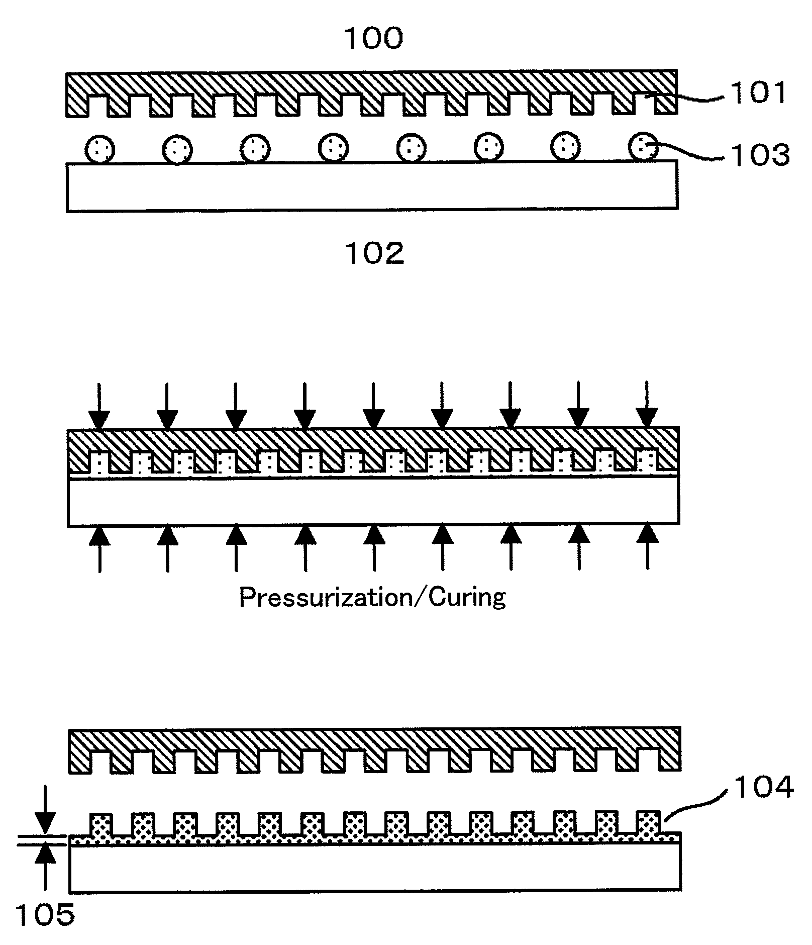
[0103]In the present example, a groove structure was formed in a disc substrate.

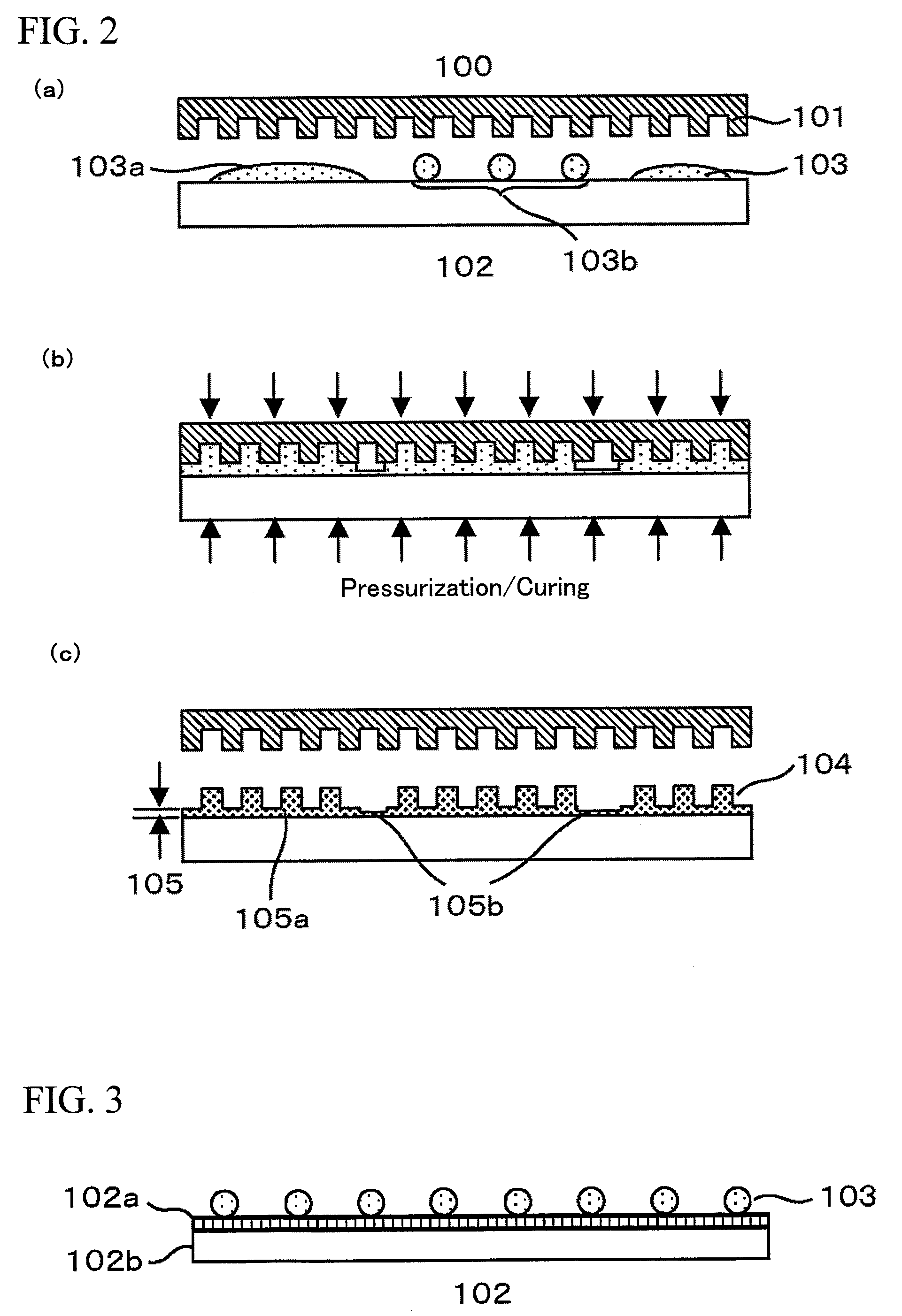
[0104]An employed substrate 102 was a discoid glass substrate having a diameter of 65 mm, a thickness of 0.6 mm, and a diameter of the center hole Hb of 20 mm. The edge part of the periphery and the edge part of the center hole in the substrate 102 were previously chamfered by a width of 0.15 mm. The substrate 102 was immersed in a solution containing 1% of phenethyl trimethoxysilane in a solvent of 2-propanol, and was heated therein at 70° C. for 1 hour. Subsequently, the substrate 102 was cleaned with 2-propanol twice, was dried, and then was dried at 120° C. for 10 minutes to obtain an intermediary layer 102a thereon with a film thickness of 1.2 nm. A resin material 103 was instilled drop-wise on the surface of the substrate 102 with an ink-jet technique right before a nanoimprint operation. The resin was an acrylate-based photo-curable resin to which a photosensitive material was added, and had a vis...

example 2

[0108]An intermediary layer was formed with the use of various silane coupling agents in a similar procedure to that in Example 1, and the fine geometry was imprinted onto the resist. The results on the film thickness and the surface roughness Ra of the base layer will now be described below. Specifically, the silane coupling agent expressed by the following chemical formula was used.

Y—Si—(OCH3)3  (Chemical Formula 2)

[0109]At first, an intermediary layer 102a was formed on the surface of a substrate of a quartz disc having a smooth surface, and the contact angle against water was evaluated. Then, the intermediary layer 102a was formed on the substrate of the quartz disc, the pattern was imprinted thereon, and the thickness of the base layer and the surface roughness Ra were evaluated. The results are shown in Table 1. In Table 1, the thickness of the base layer and the surface roughness Ra are values including the thickness of the intermediary layer 102a.

[Table 1]

[0110]

TABLE 1Resul...

example 3

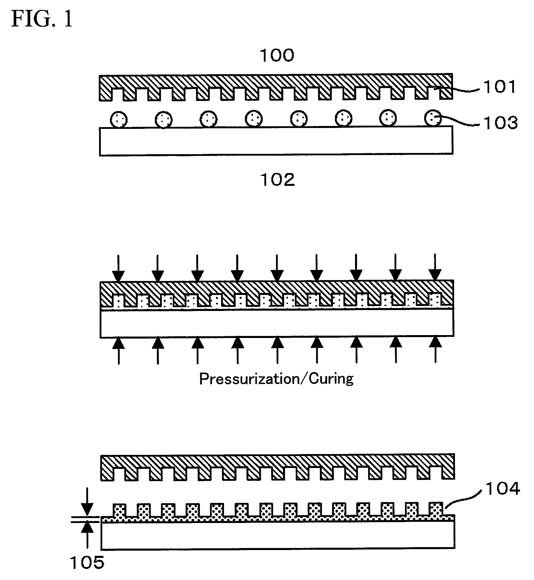
[0113]Different amounts per one droplet of a resist 103 were instilled drop-wise on the substrate by an ink-jet technique in a similar procedure to that in Example 1, and the fine geometry was imprinted onto the resist. The results on the film thickness and surface roughness Ra of the base layer will now be described below. Table 2 shows the results of the film thickness and surface roughness Ra of the base layer formed by changing the instilled amount per one droplet of the resist 103.

[Table 2]

[0114]

TABLE 2Imprint result when instilled amount per one droplet was changedInstilled amount perThickness (nm)one droplet (p1)of base layerRa (nm)0.00127460.005192150221010028125005682

[0115]When the instilled amount per one droplet of the resist 103 was 0.001 pl, the thickness of the base layer was 27 nm, the surface roughness Ra was 46 nm, and the base layer 105 caused thickness distribution therein. This was thought to be because the droplets were too small, it was difficult to control the...


PUM

PropertyMeasurementUnit
widthaaaaaaaaaa
contact angleaaaaaaaaaa

Abstract

The present invention is directed to providing a photo nanoimprint lithography which can form a more uniform base layer. A photo nanoimprint lithography according to the present invention includes the steps of discretely applying a photo-curable resist drop-wise onto a substrate, filling an asperity pattern of a mold with the photo-curable resist by bringing the mold having the asperity pattern formed therein into contact with the photo-curable resist, curing the photo-curable resist by irradiating the resist with a light and releasing from the mold the photo-curable resist which has been photo-cured, wherein an intermediary layer is formed on a surface of the substrate for maintaining a discrete placement of the photo-curable resist that has been instilled drop-wise on the substrate until the mold is brought into contact with the photo-curable resist that has been instilled drop-wise on the substrate.

Description

BACKGROUND OF THE INVENTION[0001]1. Field of the Invention[0002]The present invention relates to photo nanoimprint lithography of transferring a surface geometry of a mold onto a surface of a substrate.[0003]2. Background Art[0004]Network technology, software technology and device technology are needed to further develop due to the tendency of recent advances in information technology. To a semiconductor integrated circuit, in particular, such a high technology is required that the circuit is further refined and integrated, consequently is operated at a higher speed and is operated with low power consumption. Currently, photolithography is shifted from KrF laser lithography having the minimum line width of 130 nm to ArF laser lithography having higher resolution. However, the minimum line width of ArF laser lithography is 100 nm at a mass production level, whereas a device having the minimum line width of 45 nm is starting to be manufactured in the year 2007. In such a situation, te...

Claims


Application Information

Patent Timeline
Patent Type & Authority Applications(United States)
IPC IPC(8): B29C35/04
CPCB82Y10/00G11B5/855G03F7/0002B82Y40/00
Inventor TADA, YASUHIKOYOSHIDA, HIROSHI
Owner HITACHI LTD
Why Eureka
Try Eureka