Field Effect Transistor and Method for Manufacturing the Same

a field effect transistor and transistor technology, applied in the direction of basic electric elements, electrical equipment, semiconductor devices, etc., can solve the problems of reducing the width of the fin to approximately 10 nm or less, causing size and shape variations, and achieving the smallest possible channel width , the effect of smallest possible size and shape variation

Active Publication Date: 2009-04-09
KK TOSHIBA
View PDF3 Cites 152 Cited by
  • Summary
  • Abstract
  • Description
  • Claims
  • Application Information

AI Technical Summary

Benefits of technology

[0015]The present invention has been made in view of these circumstances, and an object thereof is to provide a field effect transistor and method for manufacturing the field effect transistor that has the smallest possible size and shape variation among channels and the smallest possible channel width.
[0016]A method for manufacturing a field effect transistor according to a first aspect of the present invention includes: forming a mask of an insulating film on a semiconductor layer containing Si formed on a semiconductor substrate; forming the semiconductor layer into a mesa structure by performing etching with the use of the mask, the mesa structure extending in a direction parallel to an upper face of the semiconductor substrate; narrowing a distance between two sidewalls of the mesa structure and flattening the sidewalls by performing a heat treatment in a hydrogen atmosphere, the two sidewalls extending in the direction and facing each other; forming a gate insulating film covering the mesa structure having the sidewalls flattened; forming a gate electrode covering the gate insulating film; and forming source and drain regions at portions of the mesa structure, the portions being located on two sides of the gate electrode.
[0017]A method for manufacturing a field effect transistor according to a second aspect of the present invention includes: forming first and second masks of insulating films on first and second semiconductor layers of Si, the first and second semiconductor layers formed in different regions from each other on a semiconductor substrate; forming the first semiconductor layer into a first mesa structure and the second semiconductor layer into a second mesa structure by performing etching with the use of the first and second masks, the first mesa structure extending in a first direction parallel to an upper face of the semiconductor substrate, the second mesa structure extending in a second direction parallel to the upper face of the semiconductor substrate; narrowing each distance between two first sidewalls of the first mesa structure and flattening the first sidewalls by performing a heat treatment in a hydrogen atmosphere, the two first sidewalls extending in the first direction and facing each other, and narrowing each distance between two second sidewalls of the second mesa structure and flattening the second sidewalls by performing the heat treatment in the hydrogen atmosphere, the two second sidewalls extending in the second direction and facing each other; forming a third mask that covers the first mesa structure and leaves the flattened second sidewalls of the second mesa structure exposed; forming a SiGe film on each of the flattened second sidewalls of the second mesa structure; performing thermal oxidization to turn the second mesa structure and the SiGe film into a third mesa structure made of SiGe and a silicon oxide film, the third mesa structure being thinner than the second mesa structure and the silicon oxide film covering sidewalls of the third mesa structure; removing the silicon oxide film; forming first and second gate insulating films covering the first and third mesa structures, respectively; forming first and second gate electrodes covering the first and second gate insulating films, respectively; forming first source and drain regions at portions of the first mesa structure, the portions being located on two sides of the first gate electrode; and forming second source and drain regions at portions of the third mesa structure, the portion being located on two sides of the second gate electrode.
[0018]A method for manufacturing a field effect transistor according to a third aspect of the present invention includes: forming first and second masks made of insulating films on a Si layer and a SiGe layer, the Si layer and the SiGe layer formed in different regions from each other on a semiconductor substrate; forming the Si layer into a first mesa structure and the SiGe layer into a second mesa structure by performing etching with the use of the first and second masks, the first mesa structure extending in a first direction parallel to an upper face of the semiconductor substrate, the second mesa structure extending in a second direction parallel to the upper face of the semiconductor substrate; narrowing each distance between two first sidewalls of the first mesa structure and flattening the first sidewalls by performing a heat treatment in a hydrogen atmosphere, the two first sidewalls extending in the first direction and facing each other, and narrowing each distance between two second sidewalls of the second mesa structure and flattening the second sidewalls by performing the heat treatment in the hydrogen atmosphere, the two second sidewalls extending in the second direction and facing each other; forming first and second gate insulating films covering the first and second mesa structures having the sidewalls flattened, respectively; forming first and second gate electrodes covering the first and second gate insulating films, respectively; forming first source and drain regions at portions of the first mesa structure, the portions being located on two sides of the first gate electrode; and forming second source and drain regions at portions of the second mesa structure, the portions being located on two sides of the second gate electrode.
[0019]A field effect transistor according to a fourth aspect of the present invention includes: a semiconductor mesa structure on a Si substrate having a {001} plane as a principal surface, having a rectangular parallelepiped shape, contains Si, having an upper face formed with a {001} plane, and having two sidewalls facing each other and being formed with {110} planes; a source region and a drain region formed at a distance from each other in a longitudinal direction of the mesa structure; a gate insulating film formed on a portion of the mesa structure, the portion being between the source region and the drain region; and a gate electrode formed on the gate insulating film, a connecting portion between each of the sidewalls of the mesa structure and the Si substrate being formed with a {111} plane.

Problems solved by technology

However, as the gate lengths have become smaller, the technical hurdle that needs to be crossed to achieve higher performances is rapidly becoming higher.
Here, there exist two technical problems: 1) size and shape variations are caused; and 2) the widths of fins need to be reduced to approximately 10 nm or less, which is smaller than the limit in terms of lithography.
The width variations result in variations in electric characteristics such as threshold voltages, and the uneven surfaces of the sidewalls cause an increase in carrier scattering and a decrease in driving current.
However, it is difficult to reduce the widths while maintaining the rectangular shapes of the fins, because of the stress in the oxide films and the dependence of the oxidation rate on the surface orientation.
By a conventional hydrogen annealing technique, however, the cross sections of the sidewalls tend to have round corners due to the surface migration.
Therefore, the conventional hydrogen annealing technique is not suitable for controlling the shapes of cross sections of Fin FETs having smaller fin widths that are required in more minute CMOS.
Furthermore, the effect of the hydrogen annealing to reduce the line edge roughness caused by the lithographic process is not clearly disclosed as technical information.
Furthermore, there has not been a report that the variation in line width was reduced by flattening the sidewalls of SiGe fins by a conventional hydrogen annealing technique.
However, it is difficult to reduce the fin widths while maintaining the rectangular shapes of the fins, due to the stress in the oxide film and the dependence of the oxidation rate on the plane direction.

Method used


Image

  • Field Effect Transistor and Method for Manufacturing the Same
  • Field Effect Transistor and Method for Manufacturing the Same
  • Field Effect Transistor and Method for Manufacturing the Same

Examples


first embodiment

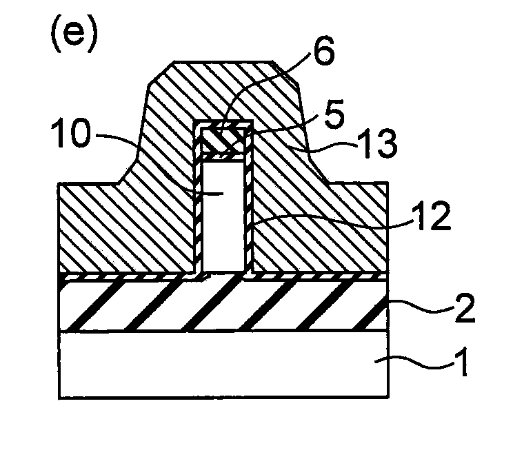
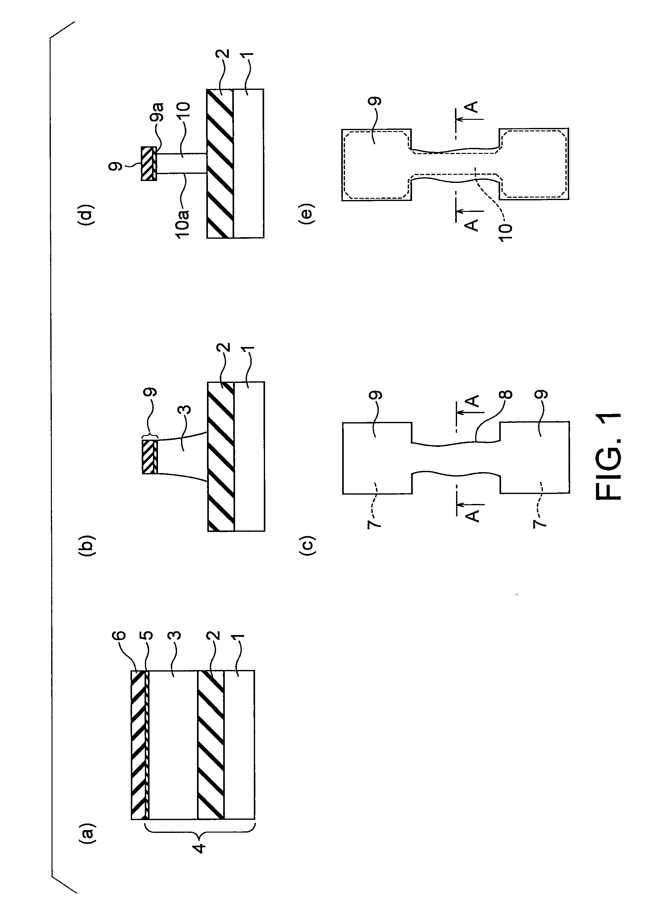
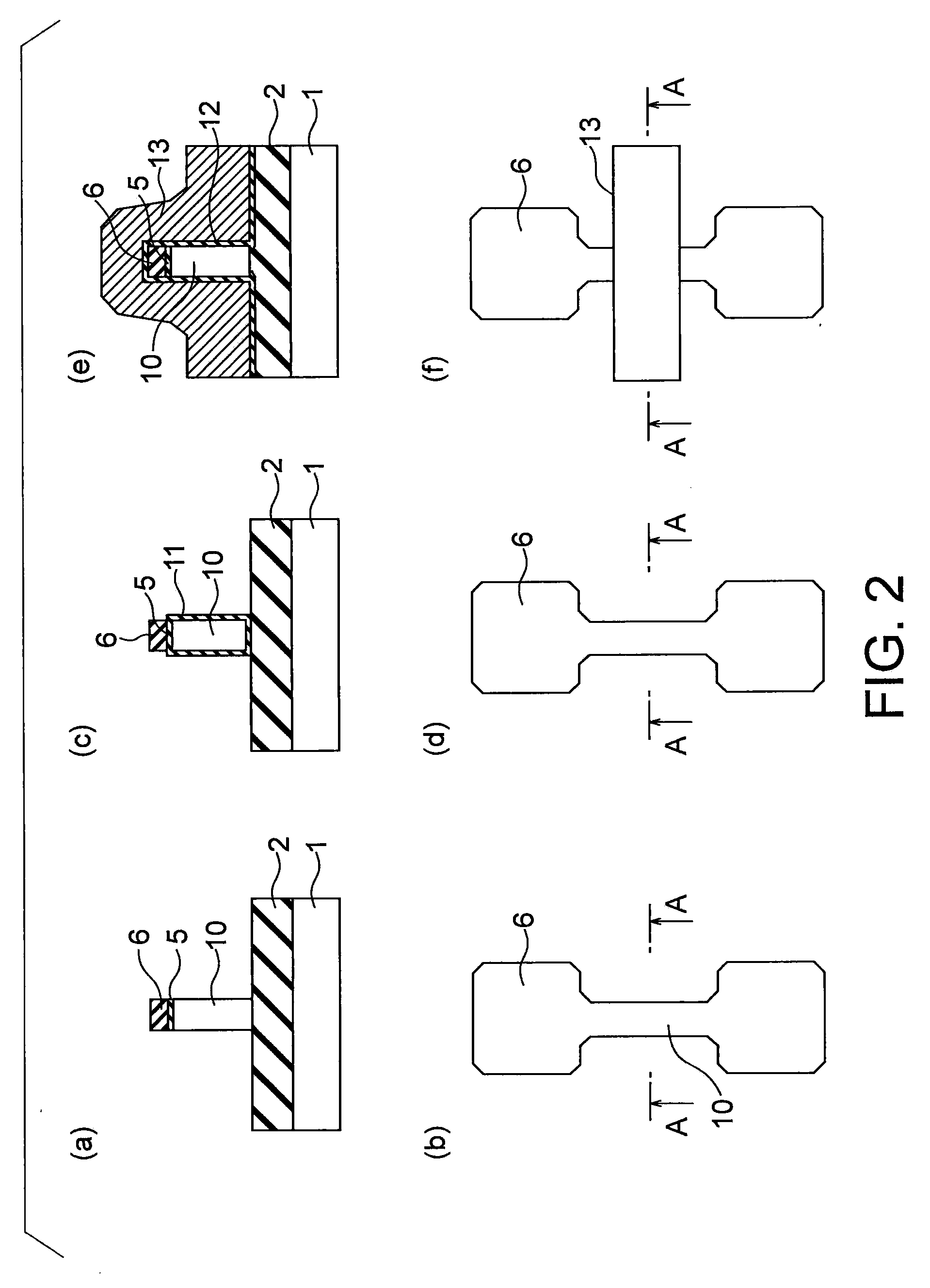
[0050]Referring to FIGS. 1(a) to 2(f), a method for manufacturing a field effect transistor in accordance with a first embodiment of the present invention is described. FIGS. 1(a), 1(b), 1(d), 2(a), 2(c), and 2(e) are cross-sectional views illustrating procedures to be carried out by the method for manufacturing the field effect transistor in accordance with this embodiment. FIGS. 1(c), 1(e), 2(b), 2(d), and 2(f) are plan views. FIGS. 1(b), 1(d), 2(a), 2(c), and 2(e) are cross-sectional views, taken along each line A-A of FIGS. 1(c), 1(e), 2(b), 2(d), and 2(f).

[0051]The field effect transistor manufactured by the manufacture method in accordance with this embodiment is a Fin FET that has a channel made of Si.

[0052]First, as shown in FIG. 1(a), a SOI substrate 4 having a supporting substrate 1, a buried oxide film 2, and a 50-nm thick SOI layer 3 having a (001) plane as the principal surface is prepared. A 2-nm thick silicon oxide film 5 and a 20-nm thick silicon nitride film 6 are d...

second embodiment

[0076]Referring now to FIGS. 4(a) to 6(f), a method for manufacturing a field effect transistor in accordance with a second embodiment of the present invention is described. FIGS. 4(a) to 4(c) are cross-sectional views illustrating the procedures to be carried out by the manufacture method in accordance with this embodiment. FIGS. 5(a), 5(c), 5(e), 6(a), 6(c), and 6(e) are cross-sectional views illustrating procedures to be carried out by the method for manufacturing the field effect transistor in accordance with this embodiment. FIGS. 5(b), 5(d), 5(f), 6(b), 6(d), and 6(f) are plan views. FIGS. 5(a), 5(c), 5(e), 6(a), 6(c), and 6(e) are cross-sectional views, taken along each line A-A of FIGS. 5(b), 5(d), 5(f), 6(b), 6(d), and 6(f).

[0077]The manufacture method in accordance with this embodiment is a method for manufacturing a nanowire MOSFET having nanowires formed with strained SiGe.

[0078]First, as shown in FIG. 4(a), a SOI substrate 4 having a supporting substrate 1, a buried oxi...

third embodiment

[0095]Referring now to FIGS. 7(a) to 7(f), a method for manufacturing a field effect transistor in accordance with a third embodiment of the present invention is described. FIGS. 7(a), 7(c), and 7(e) are cross-sectional views illustrating procedures to be carried out by the method for manufacturing the field effect transistor in accordance with this embodiment. FIGS. 7(b), 7(d), and 7(f) are plan views. FIGS. 7(a), 7(c), and 7(e) are cross-sectional views, taken along each line A-A of FIGS. 7(b), 7(d), and 7(f).

[0096]The manufacture method in accordance with this embodiment is another method for manufacturing a nanowire MOSFET having nanowires formed with strained SiGe.

[0097]First, a SOI substrate 4 having a supporting substrate 1, a buried oxide film 2, and a 30-nm thick SOI layer 3 having a (001) plane as the principal surface is prepared. The same procedures as those of the first embodiment illustrated in FIGS. 1(d) and 1(e) are then carried out. More specifically, the same proce...


PUM


Abstract

A method for manufacturing a field effect transistor, includes: forming a mask of an insulating film on a semiconductor layer containing Si formed on a semiconductor substrate; forming the semiconductor layer into a mesa structure by performing etching with the use of the mask, the mesa structure extending in a direction parallel to an upper face of the semiconductor substrate; narrowing a distance between two sidewalls of the mesa structure and flattening the sidewalls by performing a heat treatment in a hydrogen atmosphere, the two sidewalls extending in the direction and facing each other; forming a gate insulating film covering the mesa structure having the sidewalls flattened; forming a gate electrode covering the gate insulating film; and forming source and drain regions at portions of the mesa structure, the portions being located on two sides of the gate electrode.

Description

CROSS-REFERENCE TO RELATED APPLICATION[0001]This application is based upon and claims the benefit of priority from prior Japanese Patent Application No. 2007-262344 filed on Oct. 5, 2007 in Japan, the entire contents of which are incorporated herein by reference.BACKGROUND OF THE INVENTION[0002]1. Field of the Invention[0003]The present invention relates to a field effect transistor and a method for manufacturing the field effect transistor.[0004]2. Related Art[0005]Conventionally, the driving current per unit gate length is increased by reducing the gate length of each transistor and thinning each gate insulating film, so as to form more sophisticated CMOS circuit devices with higher performance. In this trend, the transistor size that can obtain the necessary driving current has become smaller, and high integration can be achieved. At the same time, the driving voltage has become lower, and the power consumption per unit device can be reduced.[0006]However, as the gate lengths hav...

Claims


Application Information

Patent Timeline
Patent Type & Authority Applications(United States)
IPC IPC(8): H01L29/778H01L21/336
CPCH01L27/1211H01L29/0673H01L29/42392H01L29/66795H01L27/1207H01L29/7842H01L29/785H01L29/78696H01L27/1203H01L29/66818H01L29/66439H01L29/775
Inventor TEZUKA, TSUTOMUTOYODA, EIJI
Owner KK TOSHIBA
Why Eureka
Try Eureka