Si-Doped GaAs Single Crystal Ingot and Process for Producing the Same, and Si-Doped GaAs Single Crystal Wafer Produced From Si-Doped GaAs Single Crystal Ingot

Inactive Publication Date: 2009-04-16
DOWA ELECTRONICS MATERIALS CO LTD
View PDF7 Cites 9 Cited by
  • Summary
  • Abstract
  • Description
  • Claims
  • Application Information

AI Technical Summary

Benefits of technology

[0016]Based on these results, the present inventors applied the method of Patent Document 3 to an Si-doped GaAs single crystal ingot, and carried out thoroughgoing research concerning the cause of reduced crystallinity in the ingot evaluated in terms of EPD. As a result, a block of GaAs raw material and a piece of Si are added to the crucible for synthesizing the raw material and B2O3 is added thereon to synthesize an Si-doped GaAs single crystal raw material in advance having the same shape as the internal shape of a crucible. It is thought that when the crucible is heated, the B2O3, which has a low melting point, becomes a liquid first, flows into the block of GaAs raw material, and makes contact with the Si piece to produce a reaction. B13As2 is generated by the reaction formula described above to form scum. This scum becomes dispersed in the Si-doped GaAs single crystal raw material, and the crystallinity of the ingot evaluated in terms of EPD is therefore ultimately reduced when the ingot is grown using the Si-doped GaAs single crystal raw material.
[0092]Adopting such a configuration allows the timing for melting the doughnut plate or another GaAs form around the dopant Si to be delayed. As a result, the average crystallinity as evaluated in terms of etch pit density can be reduced about 1 / 7, i.e., to 10 etch pits / cm2 or less in comparison with the case in which the dopant raw material is introduced into the upper portion above γ (the center interior of the GaAs raw material, where the temperature is higher than the average temperature of the GaAs compound raw material).

Problems solved by technology

However, since there is a reaction between B2O3 and the Si added as a dopant, a phenomenon occurs in which the Si concentration in the ingot becomes difficult to control.
As a result, it is difficult to consistently and stably produce an ingot having a desired favorable carrier concentration distribution.

Method used


Image

  • Si-Doped GaAs Single Crystal Ingot and Process for Producing the Same, and Si-Doped GaAs Single Crystal Wafer Produced From Si-Doped GaAs Single Crystal Ingot
  • Si-Doped GaAs Single Crystal Ingot and Process for Producing the Same, and Si-Doped GaAs Single Crystal Wafer Produced From Si-Doped GaAs Single Crystal Ingot
  • Si-Doped GaAs Single Crystal Ingot and Process for Producing the Same, and Si-Doped GaAs Single Crystal Wafer Produced From Si-Doped GaAs Single Crystal Ingot

Examples


example 1

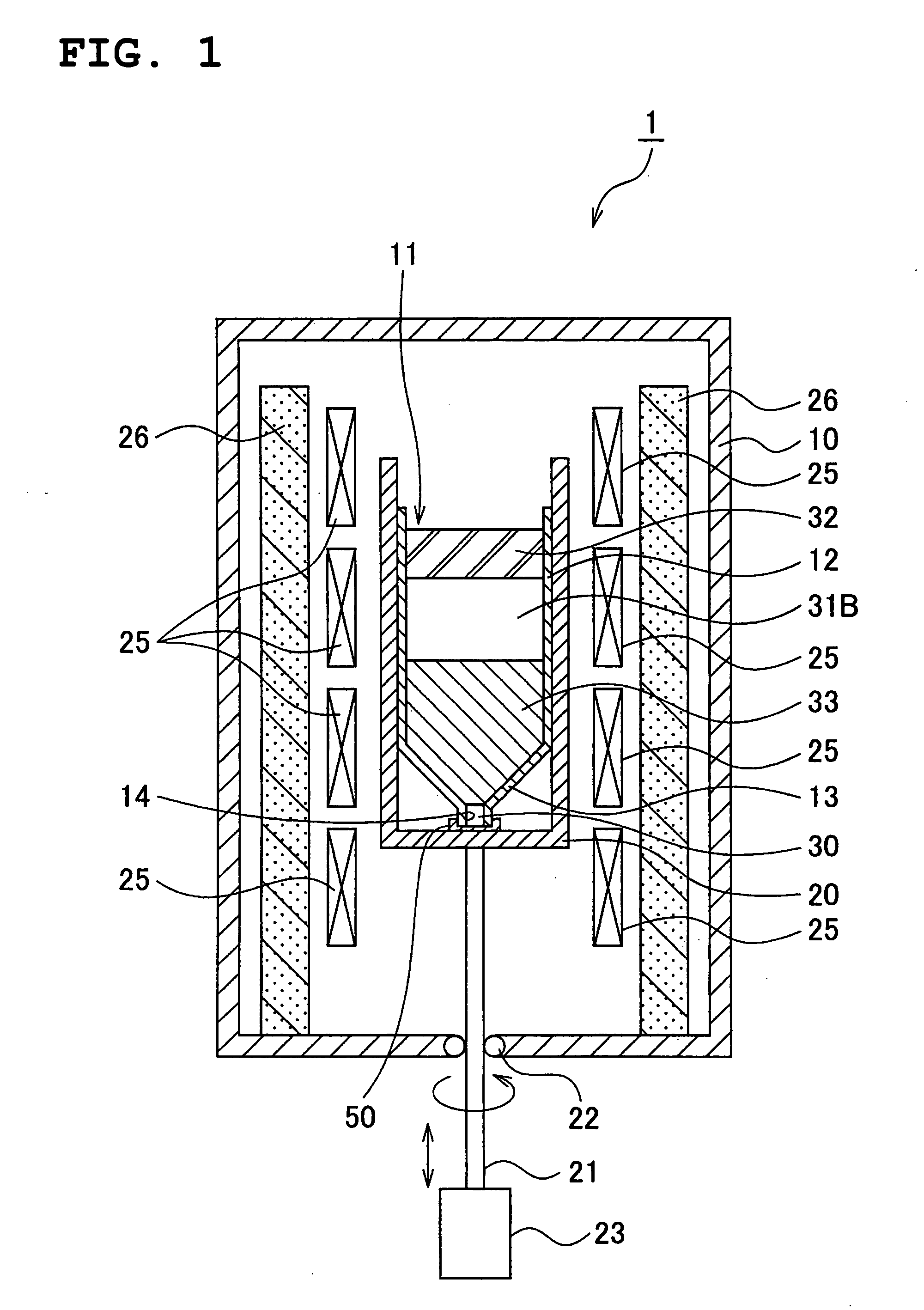
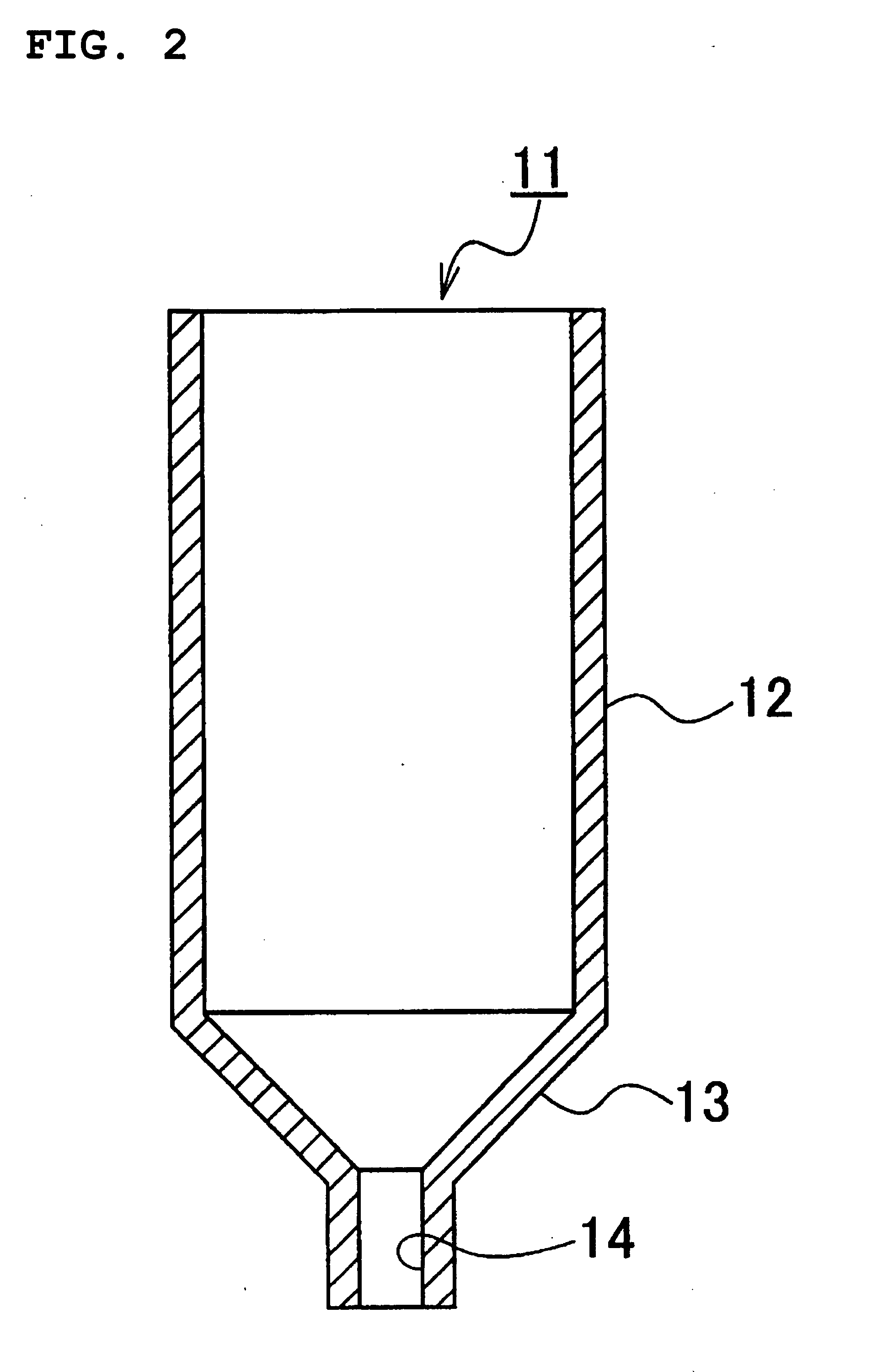
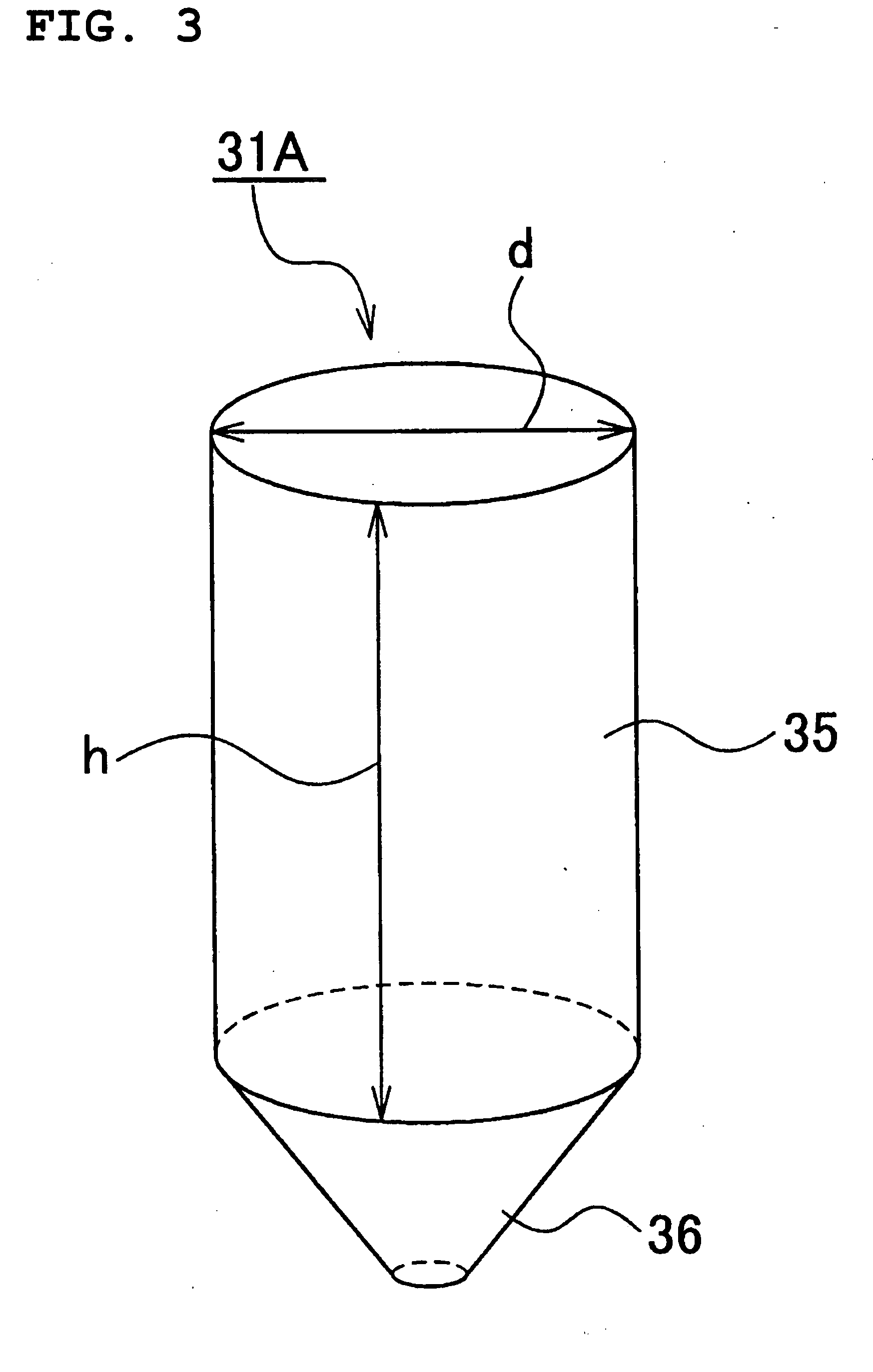
[0095]First, a GaAs compound raw material was synthesized using a separate synthesizing reactor (crucible). The value obtained by dividing the surface area of the synthesized GaAs compound raw material by the surface area of a GaAs single crystal that was grown thereafter using the GaAs compound raw material was 1.05. The synthesized GaAs compound raw material was cut and adjusted, and was furthermore cut into a cylindrical portion and a conical portion. A GaAs compound raw material in the form of a doughnut having the same outside diameter as the cylindrical portion and holding the Si dopant in the inner hole of the doughnut was inserted into the cut portion. The average temperature (ave)° C. was calculated to be 1,298° C. from the temperature profile that was used when the GaAs compound raw material described below was heated, and the insertion position was therefore located below the position that corresponds to this temperature (the temperature of the position was calculated to ...

example 2

[0102]The same apparatus and raw material as those described in example 1 were used, but the Si dopant was placed in a position at 1,327° C. rather than 1,281° C. when the dopant was inserted into the GaAs compound raw material. The same operation as in example 1 was then carried out to produce a GaAs ingot.

[0103]The carrier concentration of the resulting GaAs ingot was 0.9×10¹⁸ / cm3 in an area in which the solidification ratio was 0.1 (C0.1), the carrier concentration was 1.1×10¹⁸ / cm3 in an area in which the solidification ratio was 0.8 (C0.8), and the ratio C0.8 / C0.1 was 1.22.

[0104]The value of crystallinity evaluated in terms of etch pit density was 10 etch pits / cm2. The value obtained by dividing the fourth power of the B concentration by the cube of the Si concentration was 0.93×10¹⁹ / cm3 in the same area.

[0105]The same test as example 2 described above was carried out ten times, and the same measurements were taken. The result was C0.8 / C0.12.


PUM


Abstract

This invention provides an Si doped GaAs single crystal ingot, which has a low crystallinity value as measured in terms of etch pit density (EPD) per unit area and has good crystallinity, and a process for producing the same. An Si-doped GaAs single crystal wafer produced in a latter half part in the growth of the Si doped GaAs single crystal ingot is also provided. A GaAs compound material is synthesized in a separate synthesizing oven (a crucible). An Si dopant is inserted into the compound material to prepare a GaAs compound material with the Si dopant included therein. The position of insertion of the Si dopant is one where, when the GaAs compound material is melted, the temperature is below the average temperature. After a seed crystal is inserted into a crucible for an apparatus for single crystal growth, the GaAs compound material with the Si dopant included therein and a liquid sealing compound are introduced into the crucible. The crucible is set in the apparatus for single crystal growth, where the mixture is heat melted and, while stirring the liquid sealing compound, the melt is solidified by a vertical temperature gradient method and the crystal is grown to prepare an Si doped GaAs single crystal ingot. In this case, an Si doped GaAs single crystal wafer is also produced in the latter half part of the growth of the ingot.

Description

TECHNICAL FIELD[0001]The present invention relates to an Si-doped GaAs single crystal ingot (may hereinafter be referred to as “ingot”) for producing a GaAs single crystal wafer (may hereinafter be referred to as GaAs wafer), which is a material for a GaAs device, to a process for producing the same, and to an Si-doped GaAs single crystal wafer produced from the Si-doped GaAs single crystal ingot.BACKGROUND ART[0002]The vertical boat method (vertical gradient freeze (VGF method)) and the vertical Bridgeman method (VB method) are used to carry out crystal growth in order to produce n-type conductivity GaAs single crystal ingots for producing GaAs wafers, which are materials for GaAs (gallium arsenide) devices.[0003]In this case, Si is added as a dopant to the GaAs single crystal in order to provide a carrier to the ingot when an n-type electroconductive ingot is produced. On the other hand, there is a method in which B2O3 (boric oxide) is used as a liquid sealant for preventing As, w...

Claims


Application Information

Patent Timeline
IPC IPC(8): H01B1/06C30B28/04
CPCC30B11/00C30B27/00Y10T428/268Y10T428/24355C30B29/42
Inventor OSHIKA, YOSHIKAZU
Owner DOWA ELECTRONICS MATERIALS CO LTD
Why Eureka
Try Eureka