Digital delay locked loop circuit using mode register set

Active Publication Date: 2009-05-07
SK HYNIX INC
View PDF3 Cites 12 Cited by
  • Summary
  • Abstract
  • Description
  • Claims
  • Application Information

AI Technical Summary

Benefits of technology

[0013]Instead of using a conventional analogue method, which removes a phase difference by continuously tracking a clock through the control of a delay value for a phase locked signal between an inputted clock and a reference clock, the present invention generates a phase locked clock for determining the timing at which the data corresponding to the read command are outputted through an internal operation, by considering a CAS latency (CL) value that has beenset in a mode register set (MRS), together with a clock I/O delay time. Also, in case that the semiconductor memory device receives an error detection command for a write operation, the present invention can find out, in the same way, the timing at which data corresponding to a write command has reached an internal circuit, by using a stored write latency (WL) value, instead of the CAS latency. If an error detection operation through an error detection code (EDC) and a cyclical redundancy check (CRC) on extra information is adopted in the high-speed semiconductor memory device, the latency time to be set in the mode register set, which is corrected according to the error detection operation, is used. Therefore, in the semiconductor memory device t

Problems solved by technology

However, since the synchronous memory device did not sufficiently satisfy the required speed of inputting/outputting data, a DDR (Double Data Rate) synchronous memory device, which is capable of inputting/outputting data at a rising edge and a falling edge of a system clock, respectively, has been developed.
However, the system clock inputted to the semiconductor memory device is inevitably delayed by a clock input buffer disposed in the semiconductor memory device and a transmission line for transferring a clock to the data output circuit.
However, it is difficult to use the conventional delay locked loop circuit in a semiconductor memory d

Method used


Image

  • Digital delay locked loop circuit using mode register set
  • Digital delay locked loop circuit using mode register set
  • Digital delay locked loop circuit using mode register set

Examples


Embodiment Construction

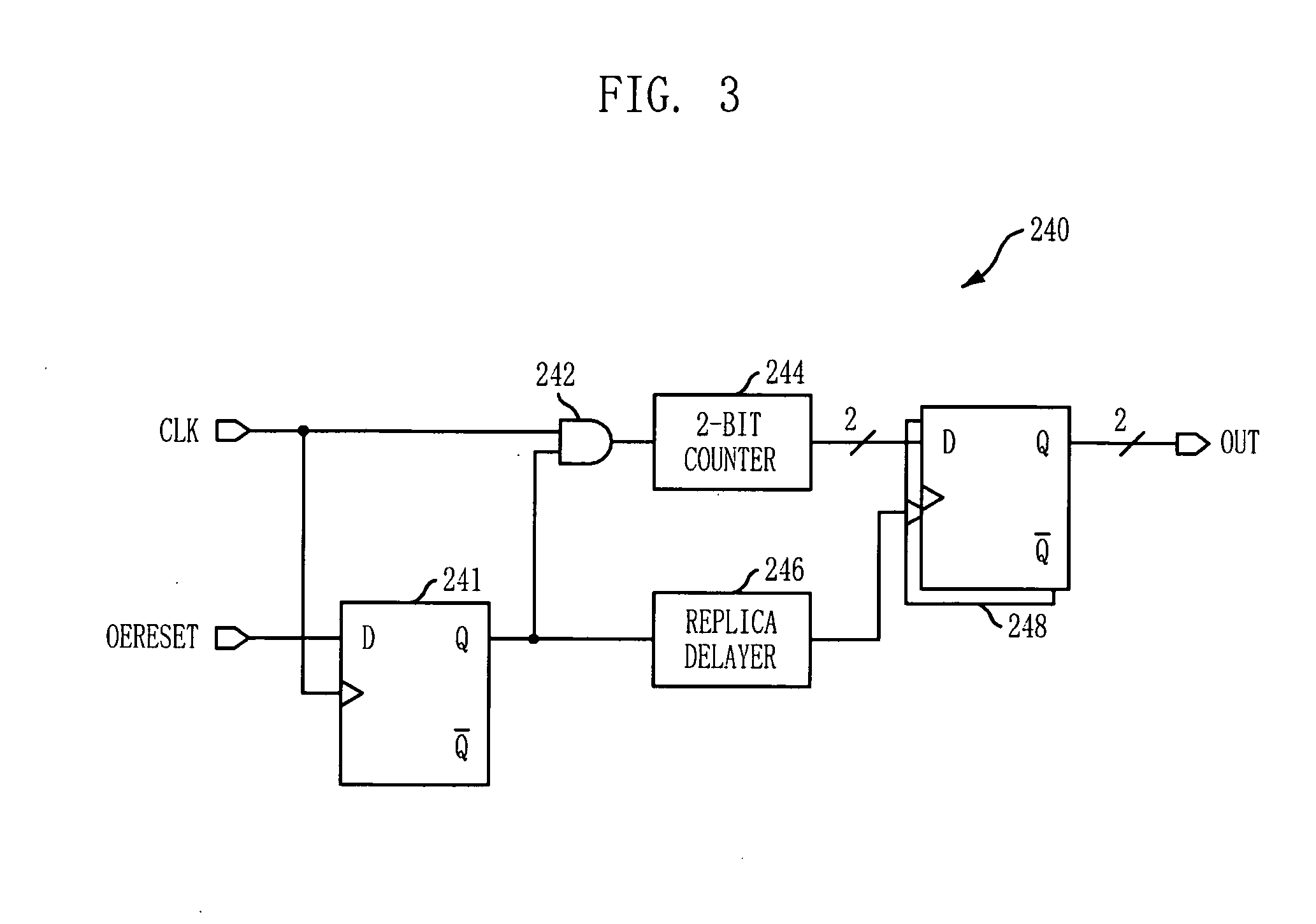
[0021]Hereinafter, the present invention will be described in detail through embodiments. The embodiments are just for exemplifying the present invention, and the scope of right to be protected of the present invention is not limited by them.

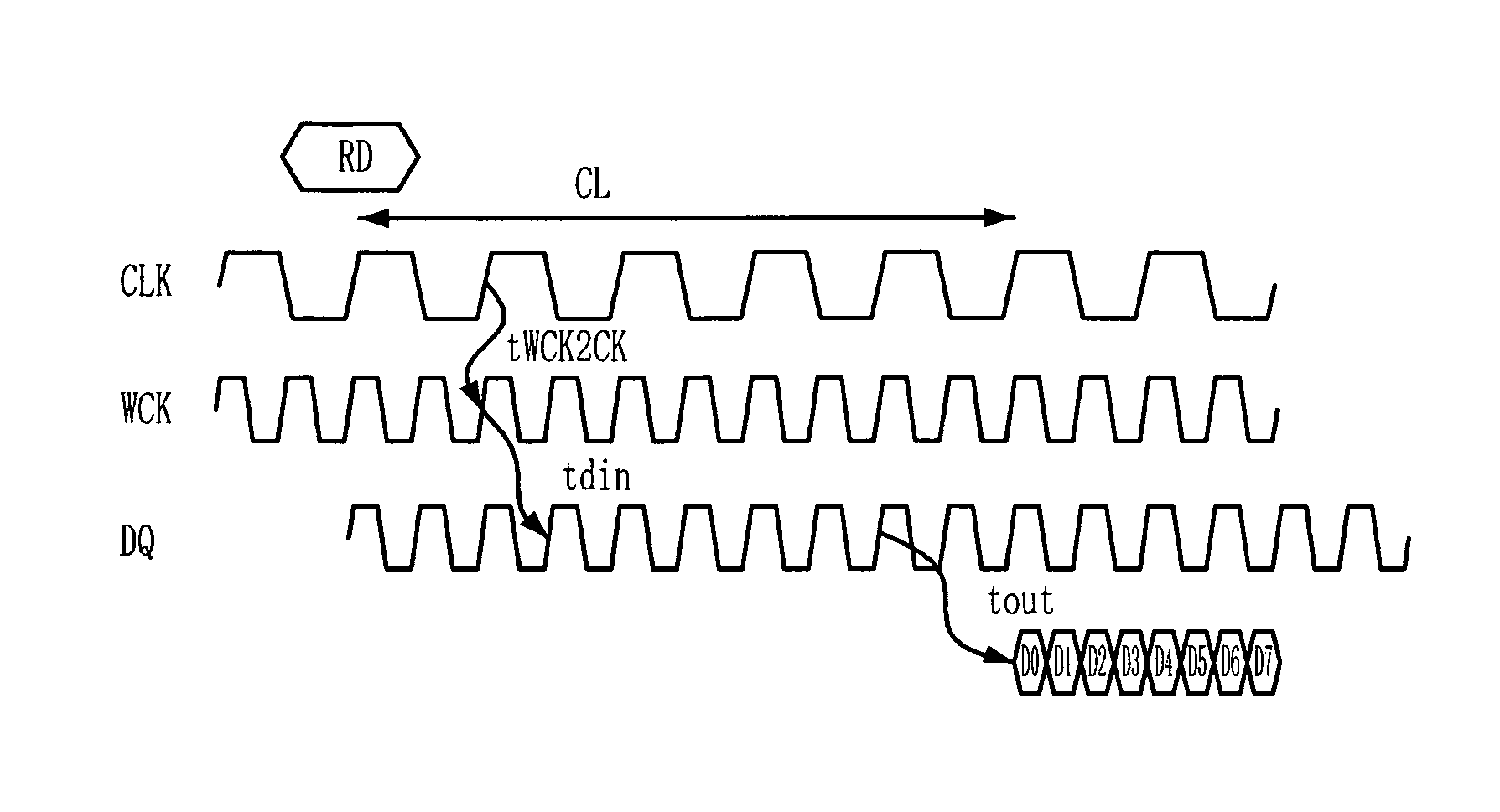
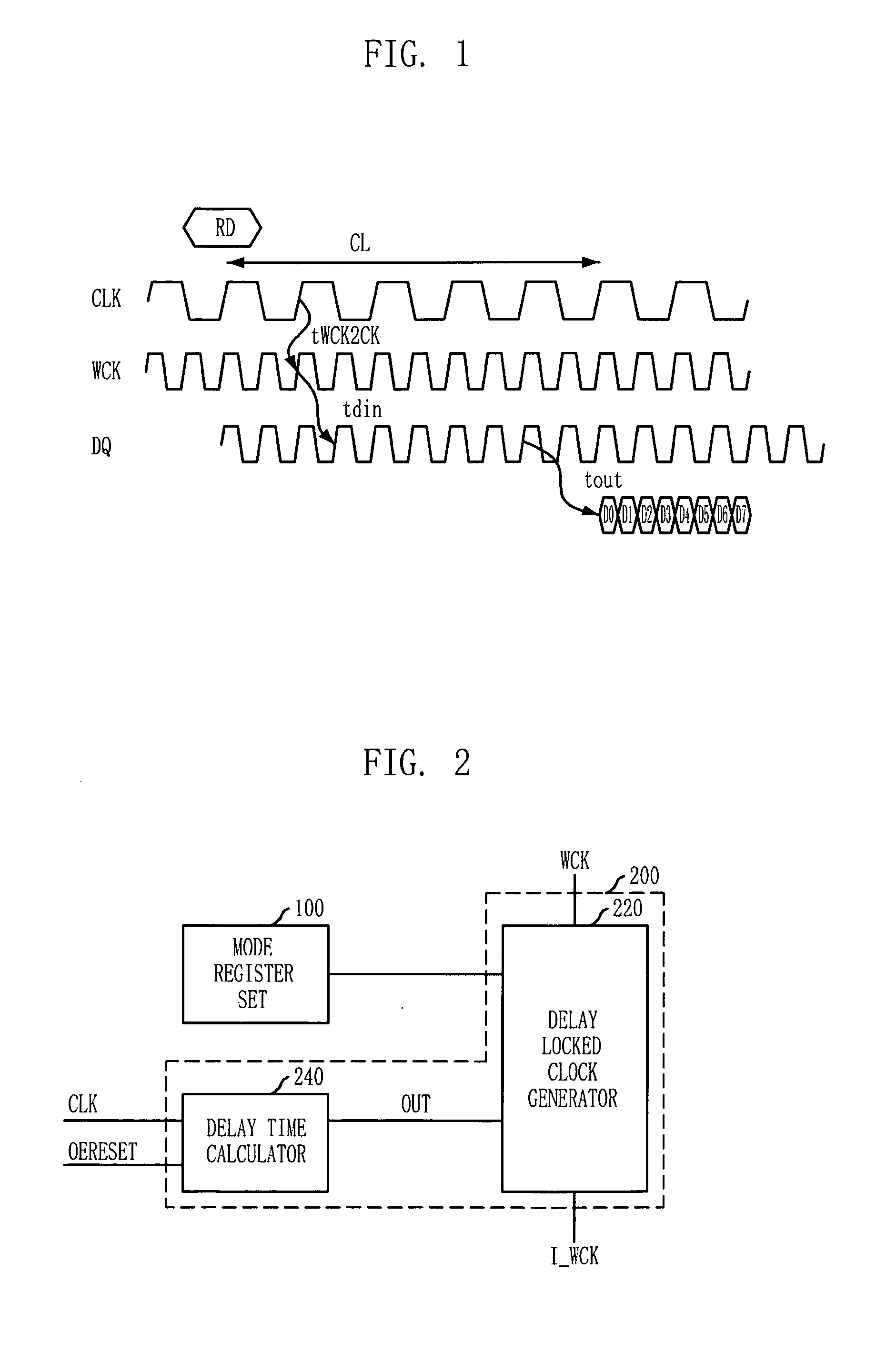
[0022]FIG. 1 is a wave form diagram showing a problem of a read operation of a conventional semiconductor memory device.

[0023]As shown in FIG. 1, the semiconductor memory device outputs data corresponding to a read command RD to an external circuit with the lapse of a predetermined time after the read command RD is inputted in synchronization with a system clock CLK. At a read operation in the semiconductor memory device, an address inputted along with the read command RD is decoded to generate an internal address and an internal command which are necessary to drive data in a unit cell corresponding to the address. Then, the semiconductor memory device senses and amplifies the data stored in the unit cell using the internal address and the inter...


PUM


Abstract

A semiconductor memory device includes a mode register set for establishing information on a delay time, a delay time calculator for calculating an I/O path delay time of a data clock on a basis of a unit period of a system clock, and a delay locked clock generator for reflecting in the data clock a value of subtracting an output of the delay time calculator from the information established in the mode register set.

Description

CROSS-REFERENCES TO RELATED APPLICATION[0001]The present application claims priority to Korean application number 10-2007-0111613, filed on Nov. 2, 2007, which is incorporated by reference in its entirety.BACKGROUND OF THE INVENTION[0002]The present invention relates to a semiconductor memory device and, more particularly, to a delay locked loop circuit for controlling an internal operation of a semiconductor memory device in order that data are outputted in synchronization with a system clock based on an external command.[0003]In a system including a plurality of semiconductor devices, the semiconductor memory device stores data. When a data processing unit, i.e., a CPU, requires data, the semiconductor memory device outputs data corresponding to an address inputted from the data processing unit or stores data provided from the data processing unit in a cell position corresponding to the address.[0004]With the increase in the operating speed of a system having semiconductor devices...

Claims


Application Information

Patent Timeline
IPC IPC(8): G06F1/12G06F1/08G06F11/07
CPCG06F11/1008G06F1/12G11C11/407
Inventor KIM, BO-KYEOMYOON, SANG-SIK
Owner SK HYNIX INC
Why Eureka
Try Eureka