Group iii nitride semiconductor crystal growing method, group iii nitride semiconductor crystal substrate fabrication method, and group iii nitride semiconductor crystal substrate
- Summary
- Abstract
- Description
- Claims
- Application Information
AI Technical Summary
Benefits of technology
Problems solved by technology
Method used
Image

Examples
first embodiment
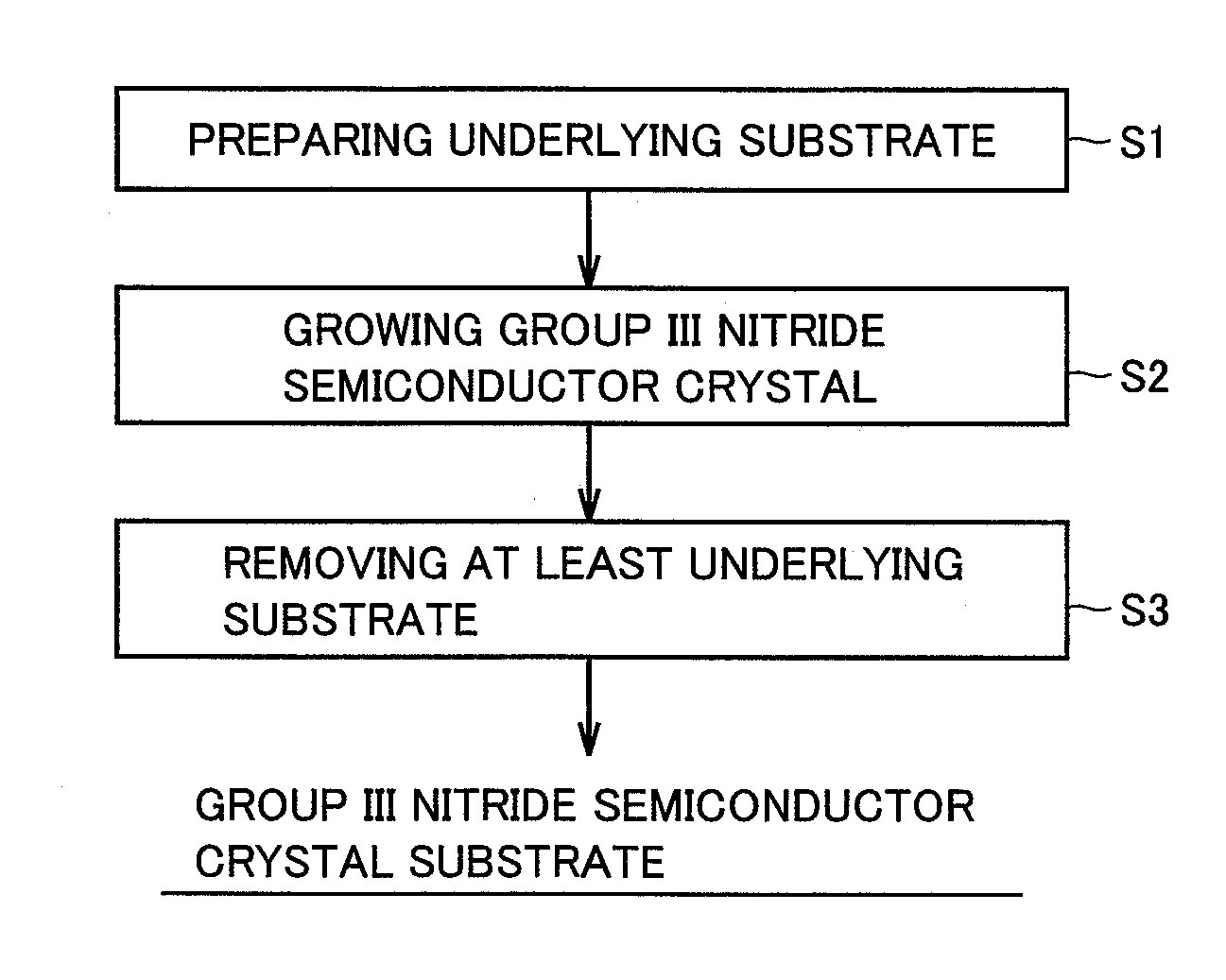
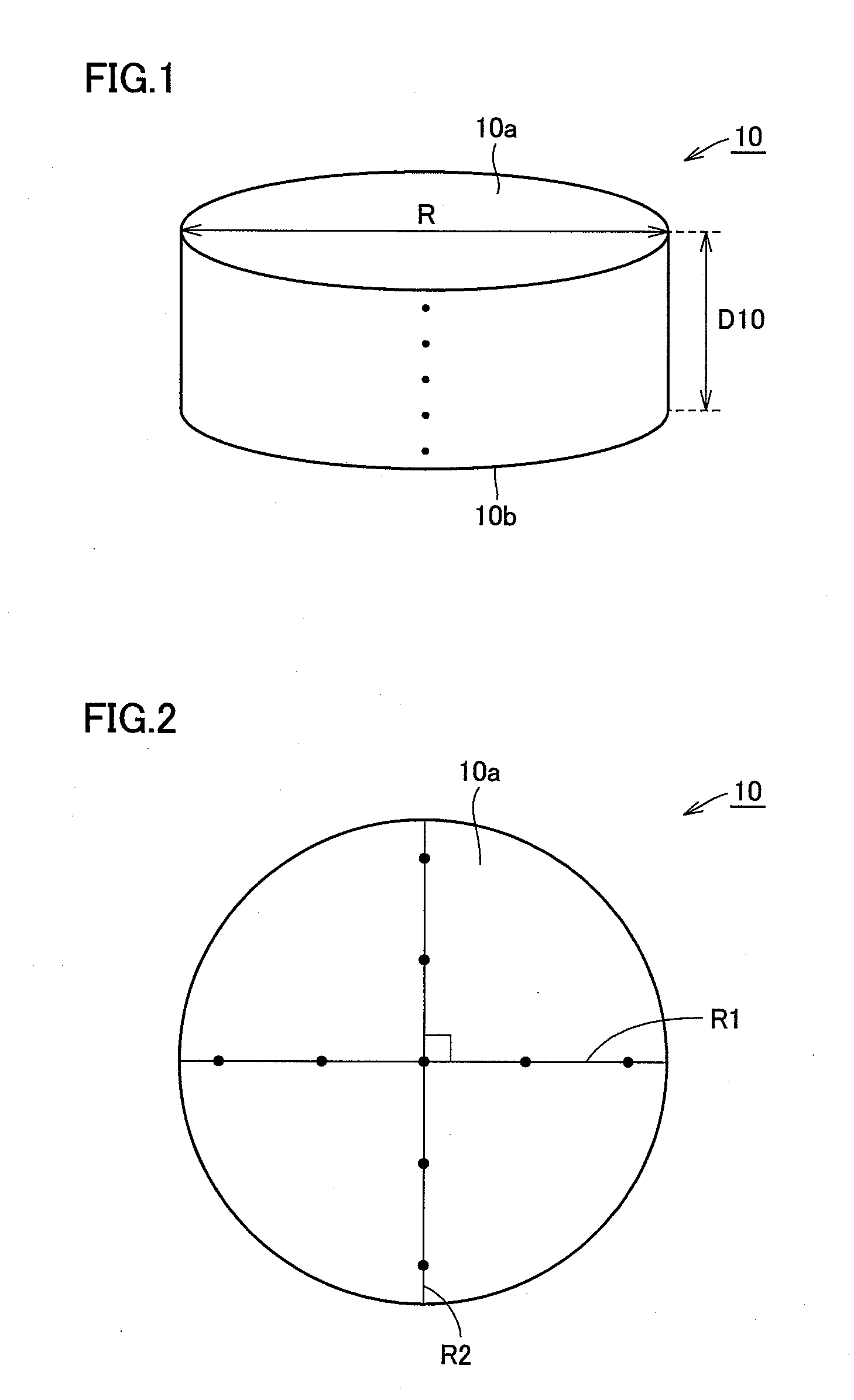
[0072]A group III nitride semiconductor crystal substrate according to an embodiment of the present invention will be described hereinafter with reference to FIGS. 1 and 2. As shown in FIGS. 1 and 2, a group III nitride semiconductor crystal substrate 10 is formed of a group III nitride semiconductor crystal 12 (refer to FIG. 4) having silicon doped as the impurity. Group III nitride semiconductor crystal substrate 10 includes a main face 10a.
[0073]As shown in FIGS. 1 and 2, a group III nitride semiconductor crystal substrate 10 of the present embodiment has a diameter R that is at least 25 mm and not more than 160 mm, preferably at least 45 mm and not more than 130 mm. A diameter R of at least 25 mm is advantageous in that the crystallinity of group III nitride semiconductor crystal substrate 10 is rendered favorable since the occurrence of a different plane orientation at main face 10a is prevented. In the case where diameter R is at least 45 mm, the crystallinity of group III ni...
second embodiment
[0147]A group III nitride semiconductor crystal substrate according to a second embodiment will be described with reference to FIG. 11.
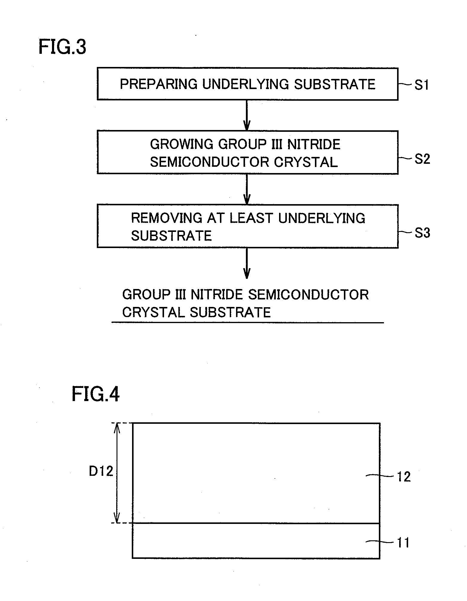
[0148]As shown in FIG. 11, a group III nitride semiconductor crystal substrate 20a of the second embodiment is basically similar to group III nitride semiconductor crystal substrate 10 of the first embodiment shown in FIG. 1. The difference lies in that thickness D20a is at least 100 μm and not more than 1000 μm.
[0149]Thickness D20a of group III nitride semiconductor crystal substrate 20a is at least 100 μm and not more than 1000 μm, preferably at least 60 μm and not more than 300 μm. In the case where thickness D20 is at least 100 μm, there can be obtained a group III nitride semiconductor crystal substrate 20a having generation of a crack during handling prevented. In the case where thickness D20a is at least 60 μm, group III nitride semiconductor crystal substrate 20a having generation of a crack further prevented is obtained. In the case where th...
example
[0162]In the present example, the effect of growing, based on the growth rate of at least 200 μm / h and not more than 2000 μm / h, a group III nitride semiconductor crystal doped with silicon, by using silicon tetrachloride gas, on an underlying substrate through vapor phase growth was evaluated. Specifically, group III nitride semiconductor crystal substrates of Specimens 1-13 were fabricated according to the second embodiment. The resistivity, the resistivity distribution in the diameter direction and thickness direction, and the silicon concentration were measured. Moreover, the surface state was observed.
[0163][Specimens 1-7]
[0164]First, an underlying substrate 11 formed of gallium nitride having a diameter of 105 mm and a thickness of 400 μm was prepared (step S1). The main face of underlying substrate 11 corresponds to the (0001) plane.
[0165]Then, a gallium nitride crystal was grown as a group III nitride semiconductor crystal doped with silicon by using silicon tetrachloride gas...
PUM
| Property | Measurement | Unit |
|---|---|---|
| Temperature | aaaaa | aaaaa |
| Temperature | aaaaa | aaaaa |
| Thickness | aaaaa | aaaaa |
Abstract
Description
Claims
Application Information
 - Generate Ideas
- Intellectual Property
- Life Sciences
- Materials
- Tech Scout
- Unparalleled Data Quality
- Higher Quality Content
- 60% Fewer Hallucinations
Browse by: Latest US Patents, China's latest patents, Technical Efficacy Thesaurus, Application Domain, Technology Topic, Popular Technical Reports.
© 2025 PatSnap. All rights reserved.Legal|Privacy policy|Modern Slavery Act Transparency Statement|Sitemap|About US| Contact US: help@patsnap.com