Silicon recycling method, and silicon and silicon ingot manufactured with that method

Inactive Publication Date: 2009-05-21
SHARP KK
View PDF10 Cites 35 Cited by
  • Summary
  • Abstract
  • Description
  • Claims
  • Application Information

AI Technical Summary

Benefits of technology

[0013]A silicon scrap, which has not been available for use due to a problem of cut of a wire of a wire saw or the like caused by inc

Problems solved by technology

High-purity silicon for a semiconductor, however, is expensive and nonconforming products are small in production quantity, and supply is thus limited.
A problem has not arisen so far because production quantity of nonconforming products of silicon for electronic devices has

Method used


Image

  • Silicon recycling method, and silicon and silicon ingot manufactured with that method
  • Silicon recycling method, and silicon and silicon ingot manufactured with that method
  • Silicon recycling method, and silicon and silicon ingot manufactured with that method

Examples


example 1

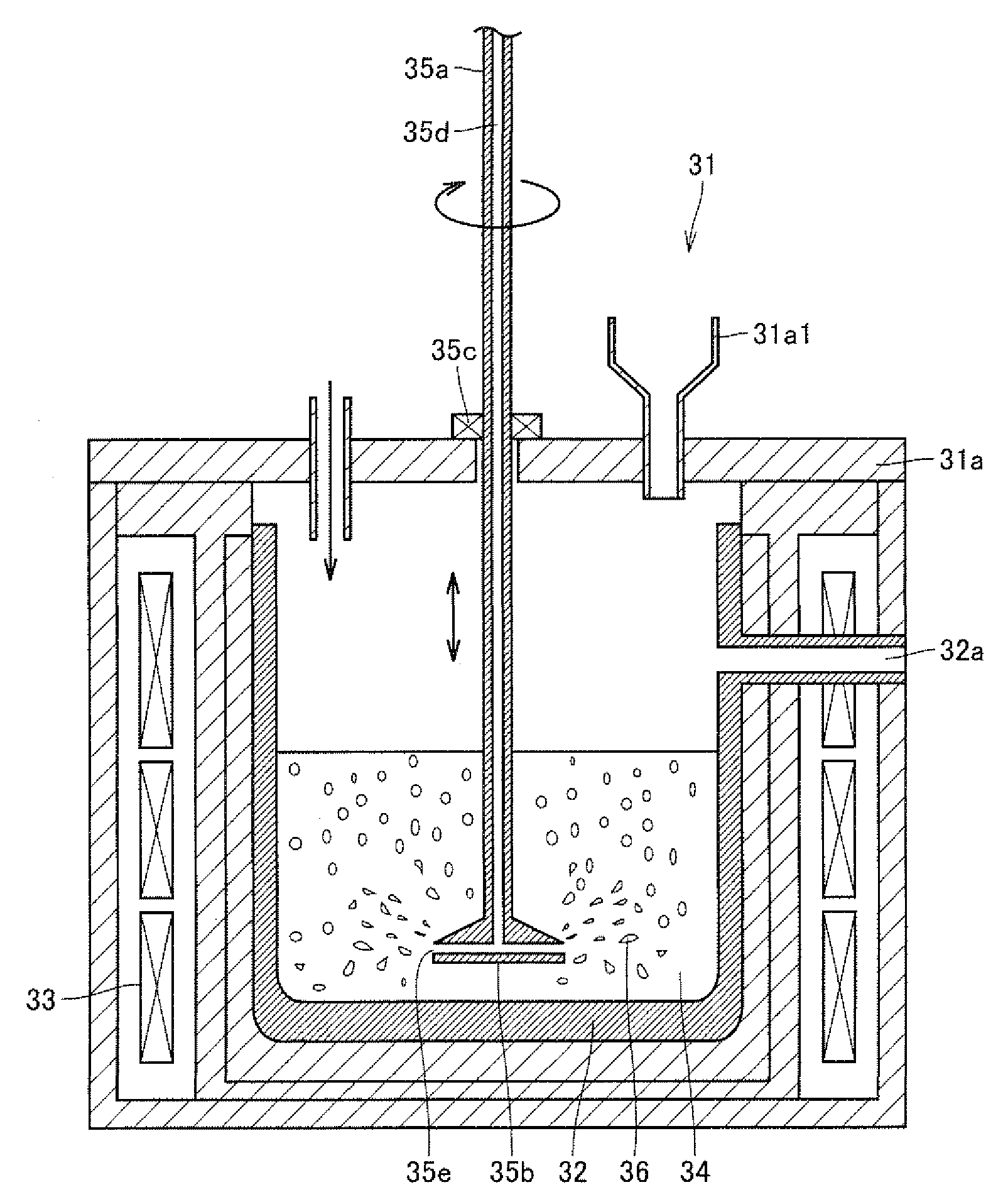
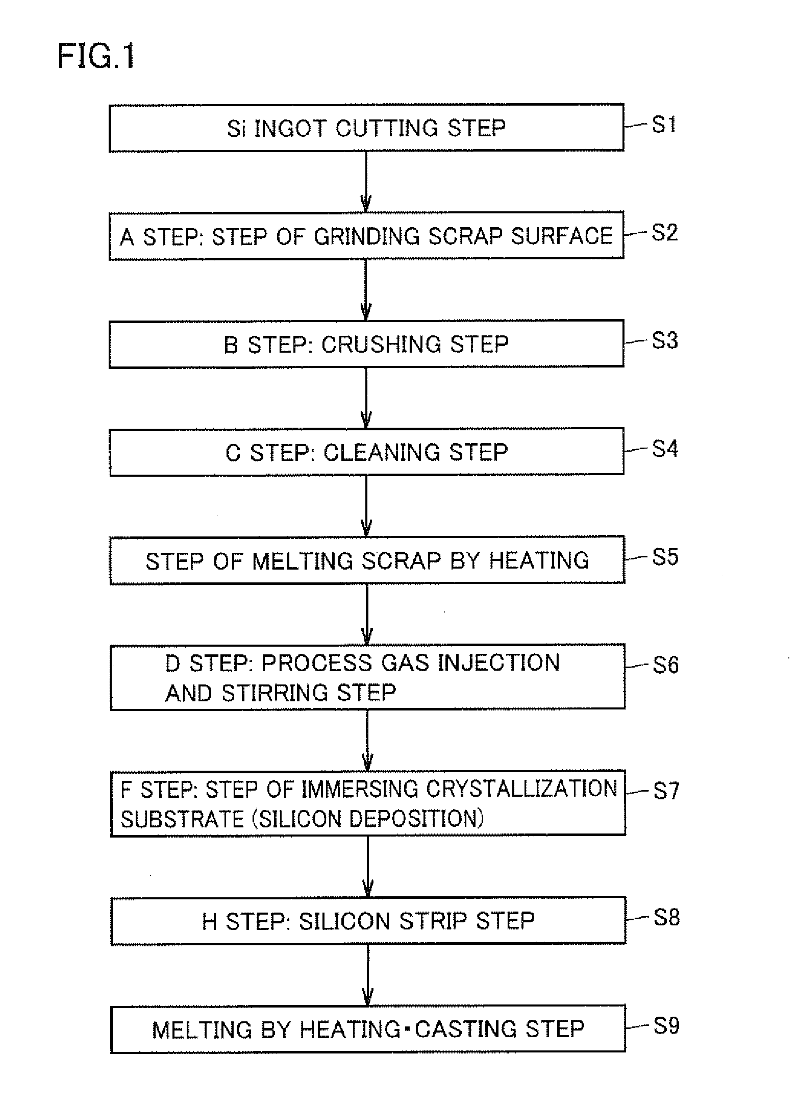
[0050]FIG. 1 is a diagram showing steps in the silicon recycling method in the present example. In the present example, as shown in FIG. 1, initially, a polycrystalline silicon ingot was cut (step 1) (hereinafter step is referred to as S). Out of removed silicon scraps, the upper surface scrap was subjected to the A step, in which the surface of the scrap was ground by approximately 3 μm with the grinder (S2). Thereafter, the B step was performed to make the size of the scrap small enough to be loaded into the crucible, and the scrap was crushed into a size from 3 to 5 cm with the jaw crusher serving as the crushing device (S3). Thereafter, the C step was performed to clean away and remove impurity such as iron on the surface of the crushed silicon raw material (S4). Cleaning was performed in such a manner that the silicon raw material was put in a stainless basket, the basket was successively passed through the surfactant bath, the water washing bath, the etching bath, and the wate...

example 2

[0057]In the present example, initially, the polycrystalline silicon ingot was cut. Out of the cut away silicon scraps removed by cutting, the upper surface scrap and the side surface scrap were used as the raw material to be processed. Then, the B step was performed to crush the raw material to be processed, such that the size thereof is small enough to be loaded into the crucible. The roll crusher was used as the crushing device and the raw material was crushed into a size from 3 to 5 cm. Thereafter, the C step was performed to remove impurity such as iron on the surface of the crushed silicon raw material, and the raw material to be processed was cleaned. Cleaning was performed in such a manner that the silicon raw material was put in a stainless basket, the basket was successively passed through the surfactant bath, the water washing bath, the etching bath, and the water washing bath each for twenty minutes while being shaken, and the silicon raw material was dried with hot air....

example 3

[0062]In the present example, the process was performed as in Example 1, except that the side surface scrap was used in addition to the upper surface scrap as the raw material silicon and that process gas injection and stirring (D step) was not performed. Here, a mass ratio between the upper surface scrap and the side surface scrap in the raw material silicon was set to 50:50. The silicon resulting from the process was cast to obtain a polycrystalline silicon ingot for solar batteries. Thereafter, the silicon ingot was cut into a block of a prescribed size with the diamond saw to obtain wafers for solar batteries each having a thickness of 200 μm. Consequently, a problem of wire cut due to foreign substances such as SiC did not arise, and it was proved that the silicon scrap is sufficiently recyclable as the raw material silicon for solar batteries.


PUM


Abstract

In order to efficiently recycle a silicon scrap obtained by cutting a silicon chunk as a raw material silicon for solar batteries, a silicon recycling method of the present invention, according to one aspect, includes the steps of melting a silicon scrap by heating, and immersing a crystallization substrate in molten silicon and depositing silicon on a surface of the crystallization substrate. The step of separating silicon on the surface of the crystallization substrate from the crystallization substrate is preferably included. In addition, a silicon ingot obtained by melting the silicon raw material for solar batteries in a mold and solidifying the same is suitable as the silicon chunk.

Description

TECHNICAL FIELD[0001]The present invention relates to a silicon recycling method. In addition, the present invention relates to silicon and a silicon ingot obtained with that method. More specifically, the present invention relates to silicon recycling by removing an inclusion and an impurity contained in a silicon scrap produced by cutting of a silicon ingot.BACKGROUND ART[0002]With growing awareness of energy issues such as exhaustion of fossil fuel resources and environmental issues such as global warming, demands for solar batteries have rapidly grown in recent years. Silicon that can be used for a solar battery cell is required to have high purity of 99.9999% or higher and specific resistance of 0.5 Ωcm or higher, and nonconforming products produced when high-purity silicon used in semiconductor industry or a substrate for an IC is manufactured are used as raw materials. High-purity silicon for a semiconductor, however, is expensive and nonconforming products are small in produ...

Claims


Application Information

Patent Timeline
IPC IPC(8): C30B9/00H01L21/00C01B33/02
CPCC01B33/021Y02E10/546C01B33/037
Inventor FUKUYAMA, TOSHIAKIOKUNO, TETSUHIROWAKUDA, JUNZO
Owner SHARP KK
Why Eureka
Try Eureka