

Preparation of A Metal-containing Film Via ALD or CVD Processes
a metal-containing film and process technology, applied in the field of metal-containing film formation, can solve the problems of increasing the difficulty of further scaling down of silicon oxide gate dielectric thickness, reducing the output of scaling, and using high-k metal oxide materials
- Summary
- Abstract
- Description
- Claims
- Application Information
AI Technical Summary
Benefits of technology
Problems solved by technology
Method used
Image

Examples
example 1
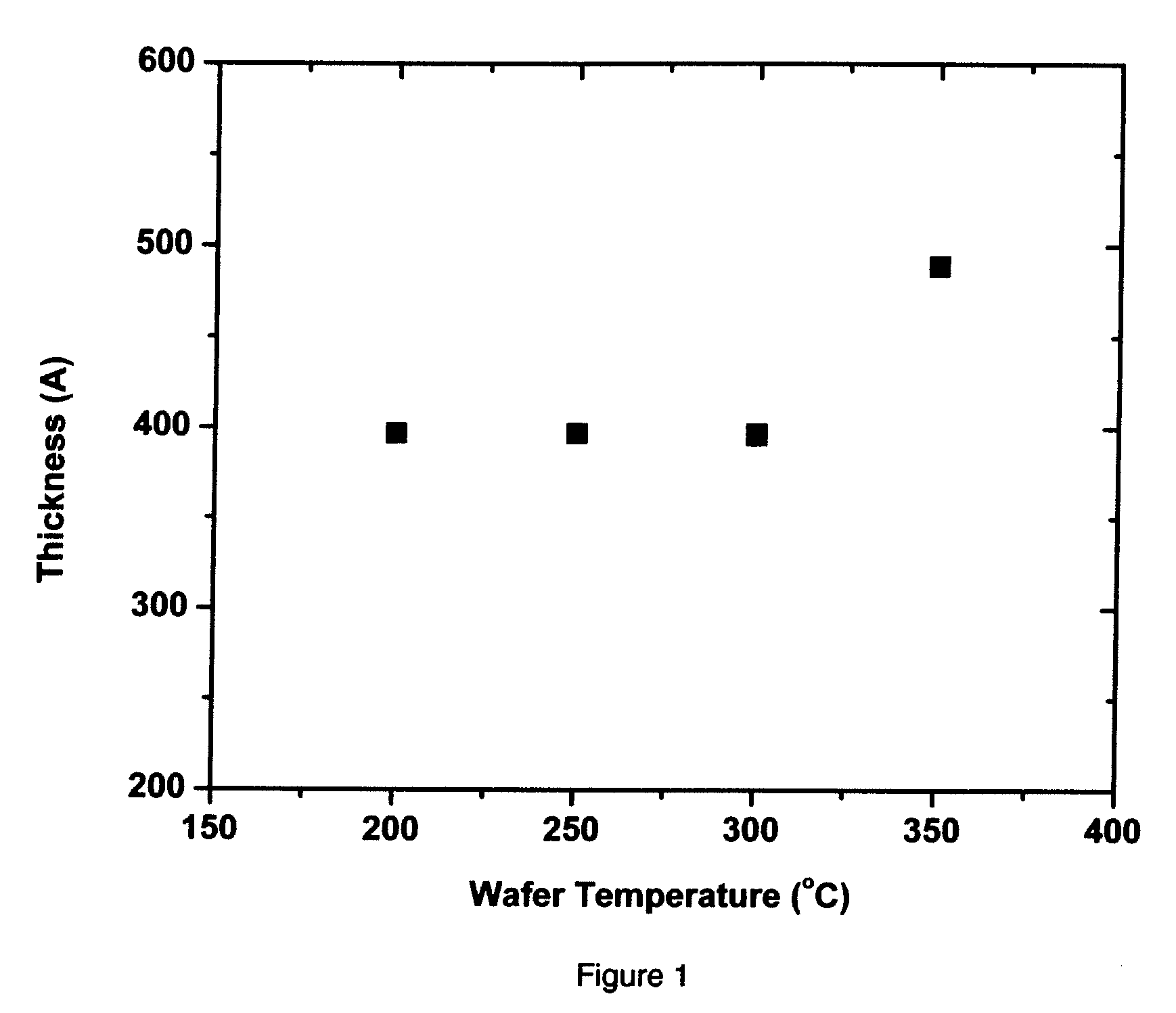
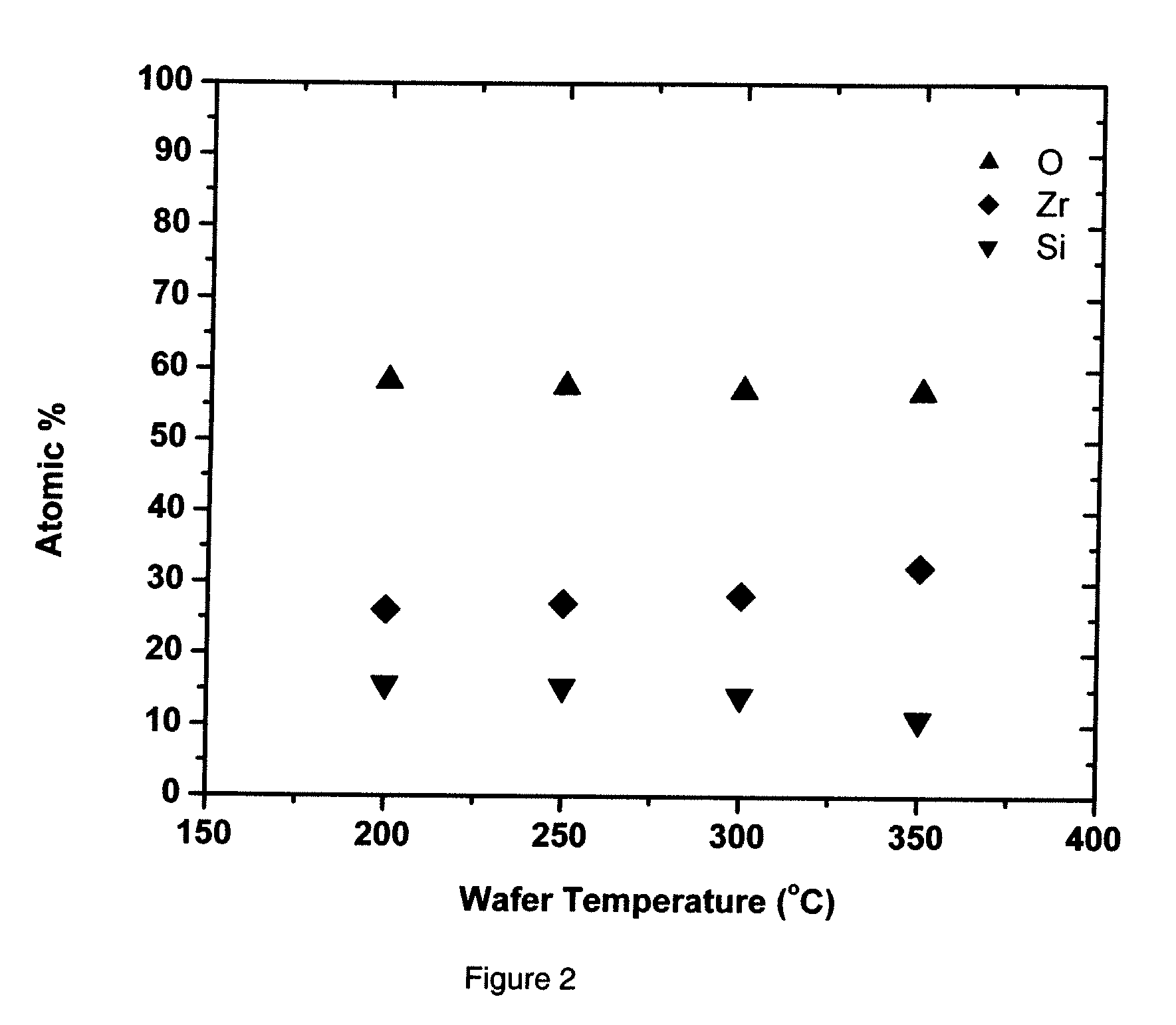
Preparation of Zirconium Silicate Films by PEALD at Various Temperatures
[0035]Exemplary zirconium silicate films were deposited in a shower-head type ALD reactor made by Quros Co. of South Korea. The temperature of the wafer was controlled using a proportional integral derivative (PID) controller. The films were deposited onto silicon wafers, which were boron-doped p-type (100) wafers having a resistivity of from 1-50 Ohm·cm, produced by LG Siltron of South Korea. The metal amide precursor used in the deposition was tetrakis(ethylmethylamino)zirconium (TEMAZ), which was housed in a temperature-controlled bubbler model BK 500 UST manufactured by Air Products and Chemicals, Inc. of Allentown, Pa. and delivered using argon as a carrier gas. The silicon-containing precursor used in the deposition was bis(tert-butylamino)silane (BTBAS) which was housed in a temperature-controlled bubbler model BK1200USH manufactured by Air Products and Chemicals, Inc. of Allentown, Pa. and delivered usin...
example 2
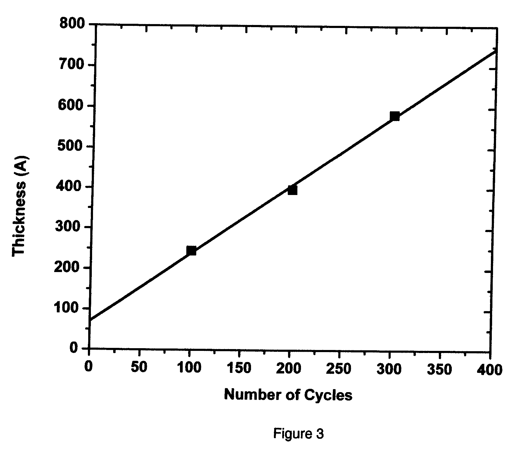
Preparation of Zirconium Silicate Films at 250° C. by PEALD
[0037]Except for the heater temperature being 250° C., three exemplary films were deposited in the same manner as described in Example 1. Wafer temperatures are 200° C., 250° C., 300° C., and 350° C. The temperature difference between wafer temperature and heater temperature was varied with heater temperature.
[0038]FIG. 3 illustrate the results of the above test. Film thicknesses of each exemplary film that was deposited at the various temperatures were measured in angstroms by spectroscopic ellipsometry using a model SE 800 spectroscopic ellipsometer manufactured by Sentech Instruments. FIG. 3 provides the comparison of film thickness versus temperature for the PEALD process for the three deposited ZrSiOx films.
example 3
Prophetic Example for the Preparation of Zirconium oxide and Silicon Oxide Nanolaminate Films at 250° C. by PEALD
[0039]Nanolaminate films comprising zirconium oxide and silicon oxide can be prepared in the following manner. Process chamber pressure is about 1.0 Torr, first of all, 200 cycles of ZrO2 were deposited with the following cycle: TEMAZ is bubbled by an Ar carrier gas at a flow rate of 25 sccm for 3 seconds; an Ar purge gas at a flow rate of 500 sccm for 5 seconds; oxygen plasma gas at a flow rate of 100 sccm for 5 seconds during RF plasma generation; and an Ar purge gas at a flow rate of 500 sccm for 5 seconds. Secondly, 50 cycles of SiO2 is deposited with the following cycle: BTBAS is bubbled by an Ar carrier gas at a flow rate of 25 sccm for 0.5 seconds; an Ar purge gas at a flow rate of 500 sccm for 5 seconds; oxygen plasma at a flow rate of 100 sccm for 5 seconds during RF plasma generation; and an Ar purge gas at a flow rate of 500 sccm for 5 seconds. Then another 200...
PUM
| Property | Measurement | Unit |
|---|---|---|
| Temperature | aaaaa | aaaaa |
| Thickness | aaaaa | aaaaa |
Abstract
Description
Claims
Application Information