Semiconductor Device and Method for Manufacturing the Same

a semiconductor device and semiconductor technology, applied in the direction of organic semiconductor devices, discharge tubes/lamp details, discharge tubes luminescnet screens, etc., can solve the problem of acceleration of deterioration of light emitting devices

Active Publication Date: 2009-05-28
SEMICON ENERGY LAB CO LTD
View PDF99 Cites 4024 Cited by
  • Summary
  • Abstract
  • Description
  • Claims
  • Application Information

AI Technical Summary

Benefits of technology

[0014]The first electrode of the invention has different number of layers depending on the parts, so that steps are formed at the boundaries between layers having different number of layers. The steps are covered with an insulator (referred to as a bank, a partition wall, mound, or the like). Incidentally, at least an upper end of the insulator is curved to have curvature radius; the curvature radius preferably 0.2 μm to 0.3 μm. The curvature radius is provided to obtain good step coverage; thus, a layer containing an organic compound or the like to be formed later can be formed with extremely thin thickness.
[0030]Further, in the case of using a structure in which a first region of a W single layer and a second region of a metal film having a stack including two layers (a W layer and an Al layer), etching can be easily conducted since the W film and the Al film has different etching rate.

Problems solved by technology

Excess current has been necessarily supplied in a light emitting element having bad light emission efficiency in order to balance the luminance of the whole light emitting surface of the light emitting device, which has been imperfection causing acceleration of deterioration of the light emitting device.

Method used


Image

  • Semiconductor Device and Method for Manufacturing the Same
  • Semiconductor Device and Method for Manufacturing the Same
  • Semiconductor Device and Method for Manufacturing the Same

Examples


embodiment mode 1

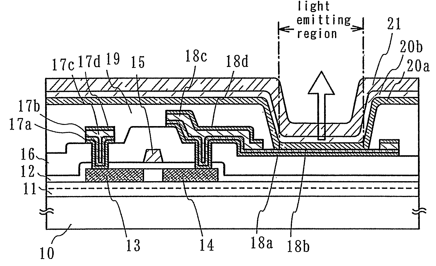
[0063]FIG. 1 is a cross-sectional view of an active matrix light emitting apparatus (a part of one pixel).

[0064]In FIG. 1, a TFT (p-channel TFT) provided over a substrate 10 having an insulating surface controls current flowing to a second EL layer 20b which emits light of blue, red, or green. Reference numerals 13 and 14 denote a source region or a drain region. A glass substrate, a plastic substrate, or the like can be used as the substrate 10. Alternatively, a semiconductor substrate or a metal substrate which has an insulating film on the surface can be used. A base insulating film 11 is formed over the substrate 10 (here, a bottom layer is a nitride insulating film and a top layer is an oxide insulating film). A gate insulating film 12 is provided between a gate electrode 15 and a semiconductor layer. Reference numeral 16 denotes an interlayer insulating film formed of with a single layer or a stack of an inorganic material, such as silicon oxide, silicon nitride, silicon nitri...

embodiment mode 2

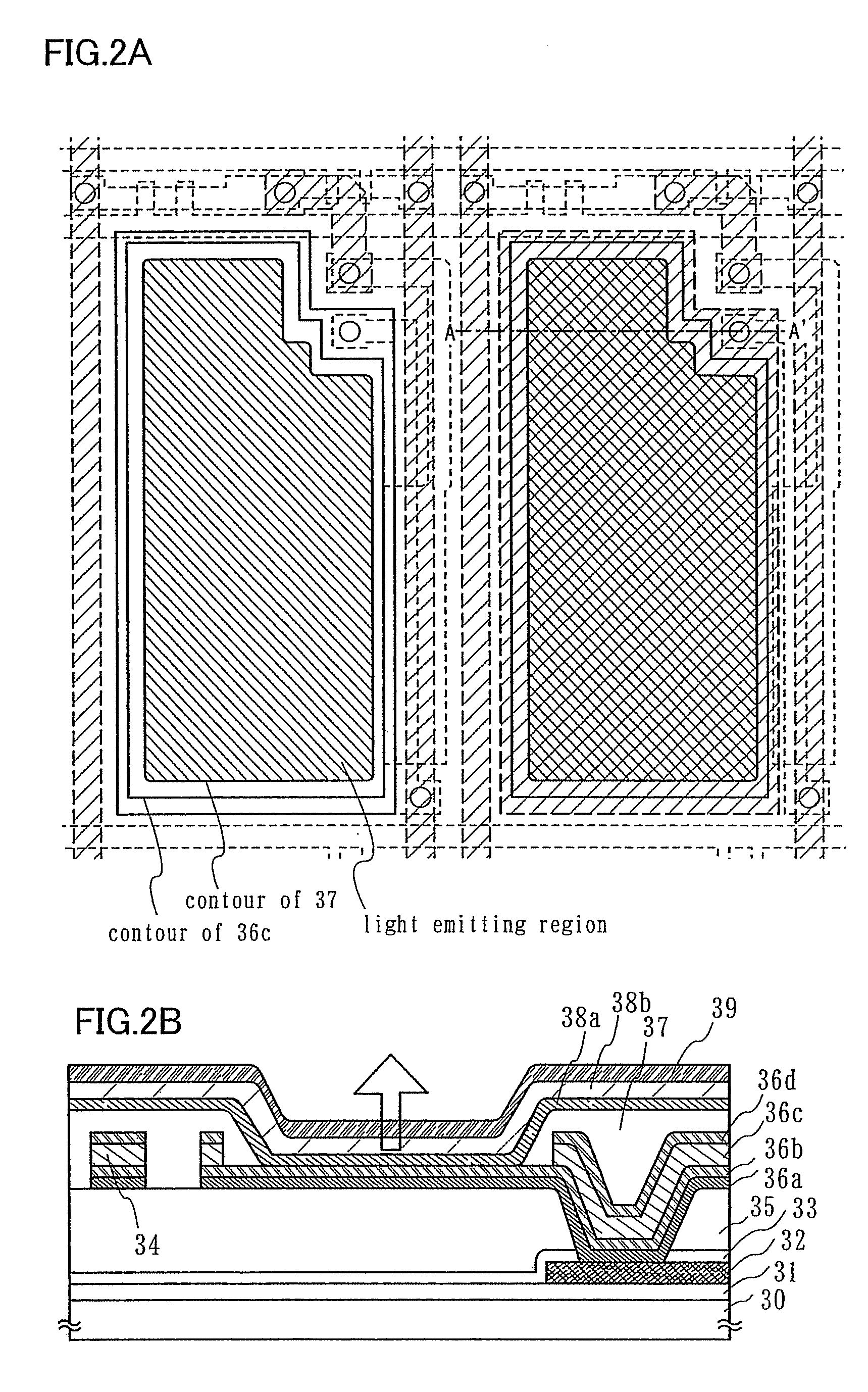
[0097]FIG. 3 shows an example of a structure according to this embodiment mode which is different from the one in Embodiment Mode 1. FIG. 3 shows a structure in which a first electrode is not directly in contact with a semiconductor layer of a TFT, but is electrically connected to the semiconductor layer of the TFT through another electrode. The first electrode has a structure in which a first region formed with a single metal layer and a second region having three layers are provided, and a step is caused between the first region and the second region. In order to improve the aperture ratio, the first region is provided at only the periphery of the contact hole, and the second region is provided in all the other regions.

[0098]In this embodiment mode, an example of forming a pixel area and a driver circuit over one substrate will be described.

[0099]First, as in Embodiment Mode 1, a base insulating film 311, a semiconductor layer formed with a crystalline semiconductor film, and a ga...

embodiment mode 3

[0125]Here, several methods for manufacturing a full-color display device will be described. Specifically, a method in which three light emitting elements are used; a method in which a white light emitting element and a color filter are used in combination; a method in which a blue light emitting element and a color conversion layer are used in combination; a method in which a white light emitting element, a color conversion layer, and a color filter are used in combination; or the like may be used.

[0126]In the case of using three light emitting elements for performing full color display, pixels each of which is provided with a red light emitting element, a blue light emitting element, and a green light emitting element, which are regularly arranged are arranged in a pixel area. For example, three kinds of evaporation masks having different opening positions for each light emission colors of R, q and B, thereby providing light emitting layers of R, G and B by vapor deposition.

[0127]...


PUM

PropertyMeasurementUnit
thickaaaaaaaaaa
thickaaaaaaaaaa
thickaaaaaaaaaa

Abstract

A manufacturing method of an active matrix light emitting device in which the active matrix light emitting device can be manufactured in a shorter time with high yield at low cost compared with conventional ones will be provided. It is a feature of the present invention that a layered structure is employed for a metal electrode which is formed in contact with or is electrically connected to a semiconductor layer of each TFT arranged in a pixel area of an active matrix light emitting device. Further, the metal electrode is partially etched and used as a first electrode of a light emitting element. A buffer layer, a layer containing an organic compound, and a second electrode layer are stacked over the first electrode.

Description

BACKGROUND OF THE INVENTION[0001]1. Field of the Invention[0002]The present invention relates to a light emitting device with a light emitting element that emits fluorescent light or phosphorescent light upon application of electric field to a pair of electrodes of the element which sandwich a layer containing an organic compound (hereinafter, an organic compound layer), and to a method of manufacturing the light emitting device. Further, the present invention relates to a deposition apparatus for forming an organic compound layer or the like.[0003]2. Description of the Related Art[0004]Light emitting elements, which use organic compounds as a light emitting member and are characterized by the thinness, lightweight, fast response, and direct current low voltage driving, are expected to be applied to next-generation flat panel displays. Among display devices, ones having light emitting elements arranged in matrix are considered to be particularly superior to conventional liquid cryst...

Claims


Application Information

Patent Timeline
Patent Type & Authority Applications(United States)
IPC IPC(8): H01L33/00H01J1/62C23C14/24H01L51/50H05B33/10
CPCH01L27/322H01L27/3244H01L27/3248H01L51/0011H01L2251/5315H01L51/5206H01L51/5218H01L51/56H01L51/5052H10K59/38H10K59/123H10K59/12H10K71/166H10K50/155H10K50/813H10K50/818H10K2102/3026H10K71/00H05B33/26H05B33/10H10K50/81
Inventor SAKAKURA, MASAYUKINODA, TAKESHIKUWABARA, HIDEAKIYAMAZAKI, SHUNPEI
Owner SEMICON ENERGY LAB CO LTD
Why Eureka
Try Eureka