Solar cell and a manufacturing method of the solar cell

a manufacturing method and solar cell technology, applied in the field of solar cells, can solve the problems of deteriorating output characteristics of solar cells, more likely to occur short circuits between substrates, etc., and achieve the effects of preventing relief structure, increasing etching rate, and high concentration

Inactive Publication Date: 2009-06-04
PANASONIC INTELLECTUAL PROPERTY MANAGEMENT CO LTD
View PDF3 Cites 44 Cited by
  • Summary
  • Abstract
  • Description
  • Claims
  • Application Information

AI Technical Summary

Benefits of technology

[0085]A manufacturing method of a solar cell 1 according to the present embodiment includes a first etching process in which the inner wall surface of the through hole is anisotropically etched, and a second etching process in which the light-receiving surface is anisotropically etched. In the first etching process, the inner wall surface of the through hole is formed to be smoother compared to the light-receiving surface. To be more specific, the first etching process uses a high concentration NaOH solution (5% by weight) and the second etching process uses a low concentration NaOH solution (1.5% by weight).
[0086]Thus, according to the manufacturing method of the solar cell 1 of the present embodiment, the etching processes can be respectively performed under different conditions, on the inner wall surface of the through hole and on the light-receiving surface. Therefore, suitable etching processes for both of the inner wall surface and the light-receiving surface can be respectively performed.
[0087]To be more specific, in the first etching process, an etching rate is increased with relatively high concentration of the etching solution, so that an over-etched state is created. As a result, a gentle relief structure having a height of zero point several μm to several μm is formed on the inner wall surface of the through hole. Meanwhile, in the second etching process, a textured structure each having a height of several μm to several tens μm suitable for a solar cell is formed.
[0088]In particular, in the present embodiment, the through hole is covered with an anti-etching mask in the second etching process. Therefore, it is possible to prevent the relief structure from being formed on the inner wall surface of the through hole in the second etching process.
[0089]As described above, on the inner wall of the through hole, the smooth surface A having arithmetic mean roughness smaller than that of the light-receiving surface is formed. On such a smooth surface A, the insulating layer 17 can be formed to have uniform thickness. Accordingly, between the n-type single-crystalline silicon 11 and the through hole electrode 20 on the smooth surface A, occurrence of the short circuit can be suppressed. As a result, the output characteristics of the solar cell 1 can be improved.
[0090]The second embodiment of the present invention will be described hereinbelow. The difference between the present embodiment and the forgoing first embodiment is that a (110) plane is exposed on the inner wall surface of the through hole, in this embodiment.

Problems solved by technology

Therefore, the insulating layer at a portion with small thickness does not sufficiently insulate the inner wall surface of the through hole and the through hole electrode from each other, and therefore a short circuit is more likely to occur between the substrate and the through hole electrode.
As a result, there has been a problem that the output characteristics of the solar cell are deteriorated.

Method used


Image

  • Solar cell and a manufacturing method of the solar cell
  • Solar cell and a manufacturing method of the solar cell
  • Solar cell and a manufacturing method of the solar cell

Examples


first embodiment

1. First Embodiment

(Schematic Configuration of Solar Cell Module)

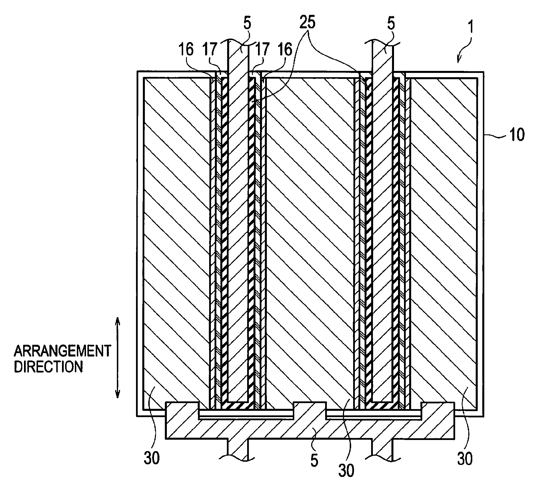
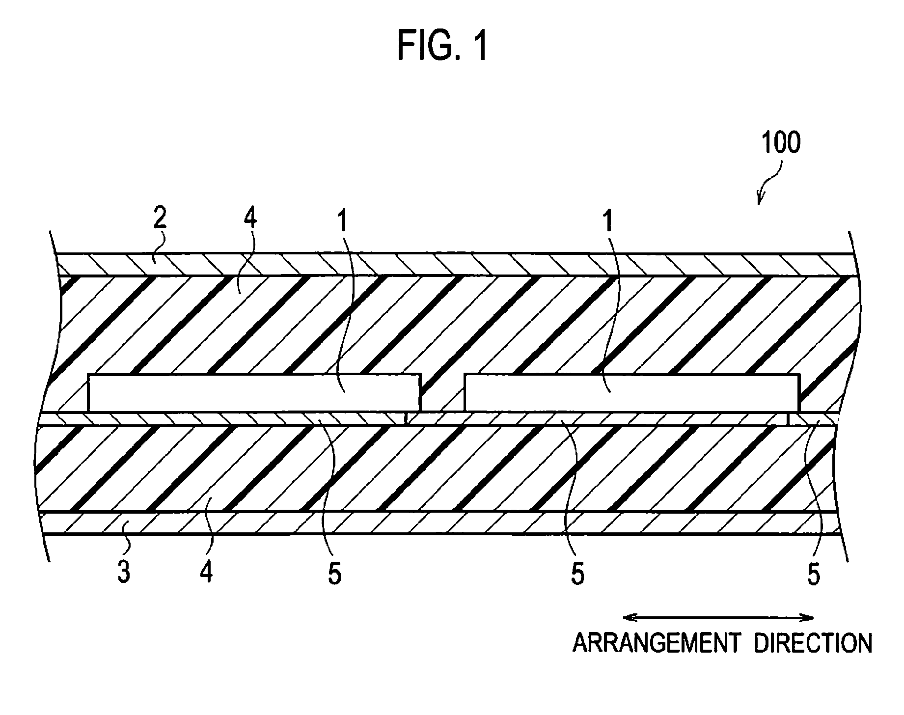
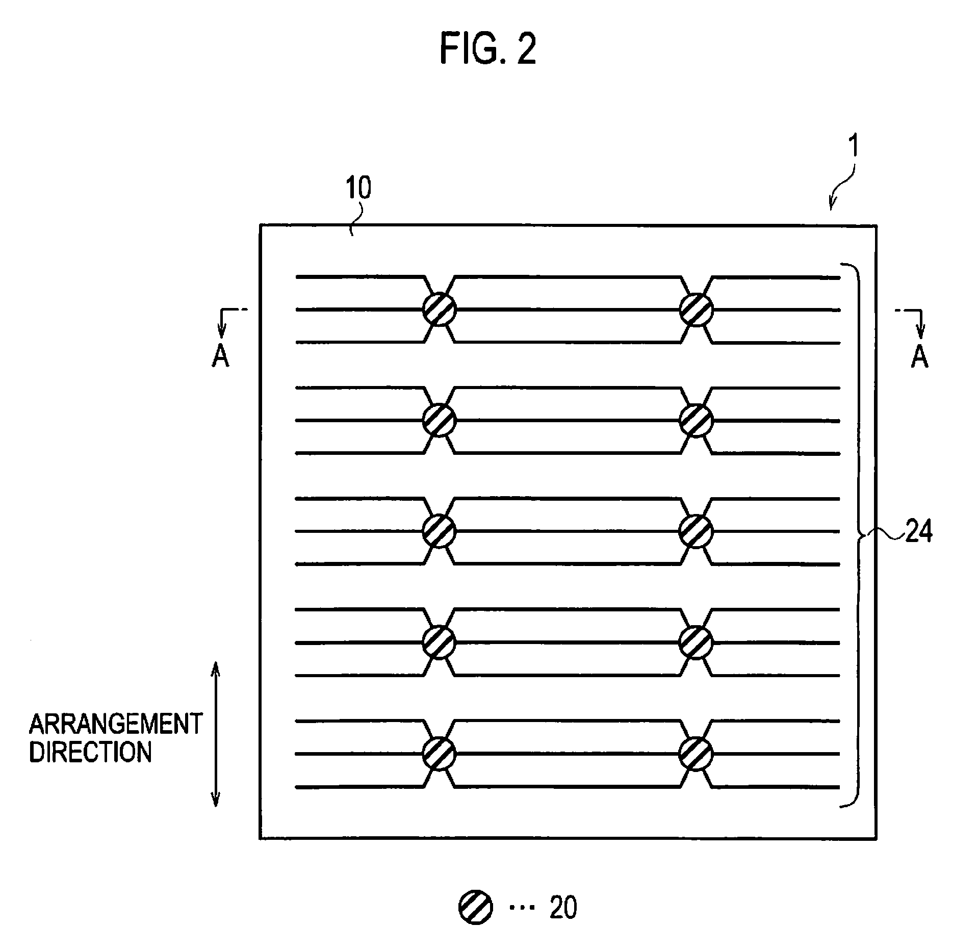
[0035]The schematic configuration of a solar cell module 100 according to the first embodiment of the present invention will be described with reference to FIG. 1. FIG. 1 is a side view showing the configuration of a solar cell module 100 according to the embodiment.

[0036]As shown in FIG. 1, a solar cell module 100 according to the embodiment includes a plurality of solar cells 1, a light-receiving-side protective member 2, a back-surface-side protective member 3, a sealing member 4, and a wiring member 5. The solar cell module 100 is formed by sealing a plurality of solar cells 1 between the light-receiving-side protective member 2 and the back-surface-side protective member 3 by using the sealing member 4.

[0037]The plurality of solar cells 1 is arranged in an arrangement direction. The plurality of solar cells 1 is electrically connected to each other through the wiring member 5. Each solar cell 1 has a light-receivi...

second embodiment

2. Second Embodiment

[0090]The second embodiment of the present invention will be described hereinbelow. The difference between the present embodiment and the forgoing first embodiment is that a (110) plane is exposed on the inner wall surface of the through hole, in this embodiment.

[0091]In the present embodiment, the schematic configurations of the solar cell module and the solar cell are the same as in the first embodiment. Accordingly, the difference from the forgoing first embodiment will mainly be described below.

(Configuration of Semiconductor Substrate)

[0092]The configuration of the n-type single-crystalline silicon 11 will be described with reference to FIG. 6. FIG. 6 is a perspective view of the n-type single-crystalline silicon 11 according to the present embodiment viewed from the light-receiving surface-side.

[0093]The light-receiving surface of the n-type single-crystalline silicon 11 is a (100) plane. As shown in FIG. 6, a textured structure is formed on the light-recei...

third embodiment

3. Third Embodiment

[0118]The third embodiment of the present invention will be described hereinbelow. The difference between the present embodiment and the forgoing first embodiment is that a semiconductor substrate mainly composed of polycrystal silicon is used in this embodiment.

[0119]In the present embodiment, the schematic configurations of the solar cell module and the solar cell are the same as in the first embodiment. Accordingly, the difference from the forgoing first embodiment will mainly be described below.

(Configuration of Photoelectric Conversion Part)

[0120]The detailed configuration of the photoelectric conversion part 50 of a solar cell la according to the present embodiment will be described with reference to FIG. 7. FIG. 7 is an enlarged cross-sectional view of the solar cell la according to the present embodiment.

[0121]The photoelectric conversion part 50 includes an n-type polycrystalline silicon substrate 51, a p-type polycrystal silicon layer 52, an anti-reflect...


PUM

PropertyMeasurementUnit
thicknessaaaaaaaaaa
thicknessaaaaaaaaaa
thicknessaaaaaaaaaa

Abstract

The manufacturing method of the solar cell according to the present invention includes: 1) a first etching process in which an anisotropic etching is performed on an inner wall of each of a plurality of through holes, and 2) a second etching process in which an anisotropic etching is performed on a light-receiving surface. In the first etching process, a high concentration NaOH water solution (about 5% by weight) is used. Meanwhile, in the second etching process, a low concentration (about 1.5% by weight) NaOH water solution is used.

Description

CROSS REFERENCE TO RELATED APPLICATIONS[0001]This application is based upon and claims the benefit of priority from prior Japanese Patent Application No. 2007-311586, filed on Nov. 30, 2007; the entire contents of which are incorporated herein by reference.BACKGROUND OF THE INVENTION[0002]1. Field of the Invention[0003]The present invention relates to a solar cell provided with a through hole electrode, and a manufacturing method of such solar cell.[0004]2. Description of the Related Art[0005]A solar cell can directly convert the clean and inexhaustibly supplied sunlight to electricity, and thus is expected as a new energy source.[0006]Conventionally, for a purpose of increasing the light-receiving surface area of the solar cell, a back contact type solar cell has been proposed in which both a p-side electrode and an n-side electrode are provided on the back-surface-side of the substrate (for example, Japanese Unexamined Patent Application Publication No. Hei 1-82570).[0007]Such a s...

Claims


Application Information

Patent Timeline
Patent Type & Authority Applications(United States)
IPC IPC(8): H01L31/042H01L31/04H01L21/31H01L31/0224H01L31/036H01L31/0747
CPCH01L31/03762H01L31/0747H01L31/02363Y02E10/548H01L31/02245H01L31/077Y02E10/546
Inventor KINOSHITA, TOSHIHIRO
Owner PANASONIC INTELLECTUAL PROPERTY MANAGEMENT CO LTD
Why Eureka
Try Eureka