Electro-absorption modulator with broad optical bandwidth

Inactive Publication Date: 2009-06-11
INTENSE LTD
View PDF17 Cites 7 Cited by
  • Summary
  • Abstract
  • Description
  • Claims
  • Application Information

AI Technical Summary

Benefits of technology

[0027]It will be understood that the device may be manufactured on a semi-insulating substrate to improve the high frequency response of the modul

Problems solved by technology

There is a trade-off between chirp, insertion loss and modulation depth that means such devices have a limited wavelength range of operation.
This limits the range of wavelengths o

Method used


Image

  • Electro-absorption modulator with broad optical bandwidth
  • Electro-absorption modulator with broad optical bandwidth
  • Electro-absorption modulator with broad optical bandwidth

Examples


Embodiment Construction

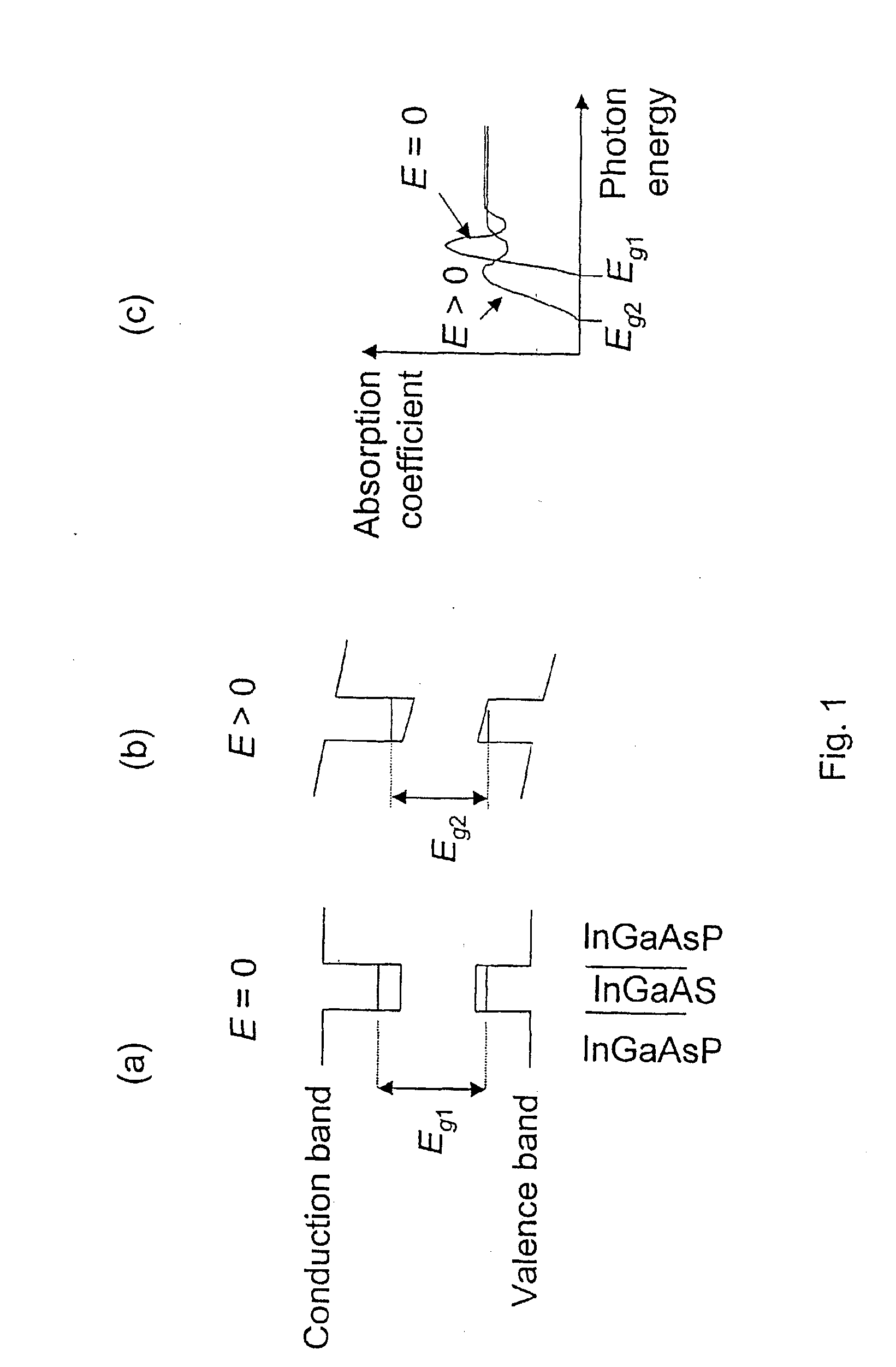
[0033]FIG. 1 illustrates the principle of the quantum confined Stark effect. For the purposes of illustration, it is assumed that the QW is composed of InGaAs and the barriers of InGaAsP. In a QW structure, the effective bandgap is determined by the fundamental material bandgap of the QW and the quantization energies of the electron and hole levels. The effective bandgap, Eg1, is shown in FIG. 1 (a). When an electric field is applied to the device perpendicular to the well (FIG. 1 (b)), the effective bandgap is reduced (Eg2), and the absorption spectrum changes (FIG. 1 (c)). The change in the absorption causes a change in refractive index spectrum.

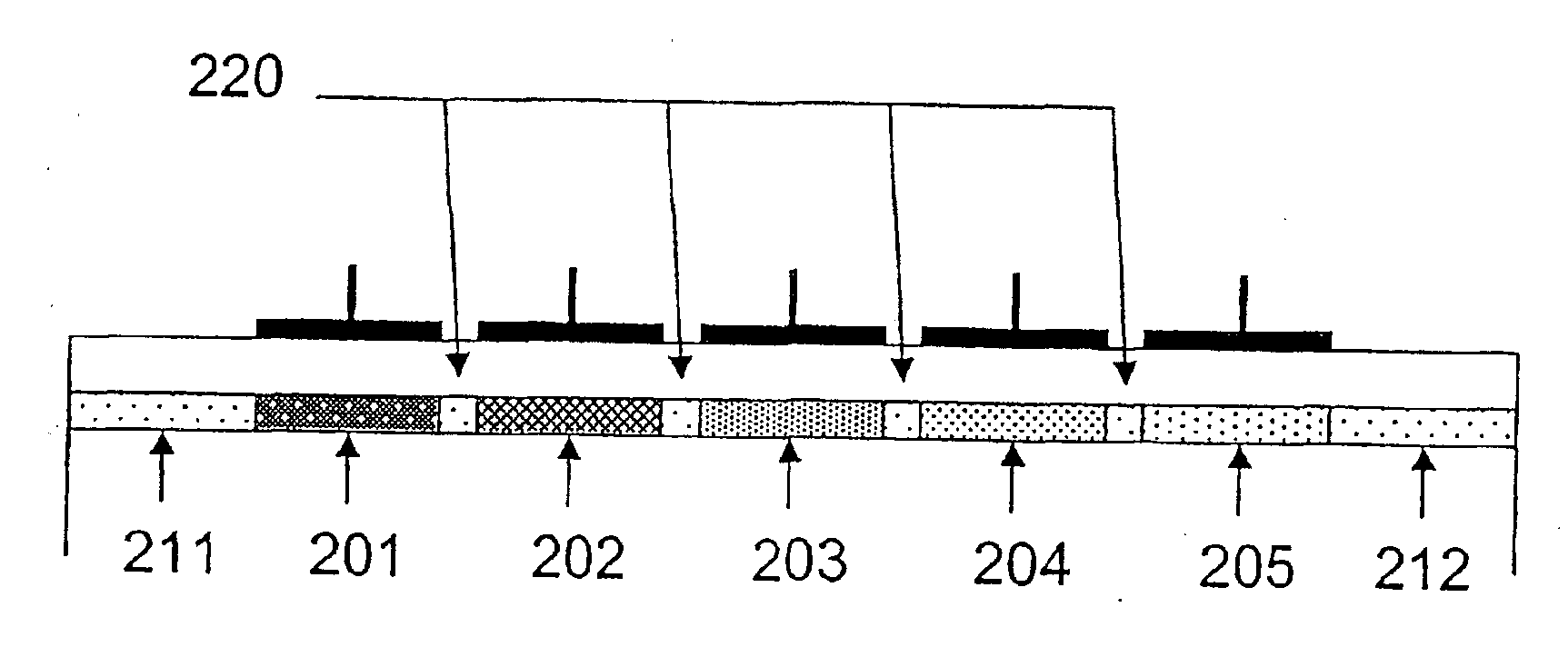
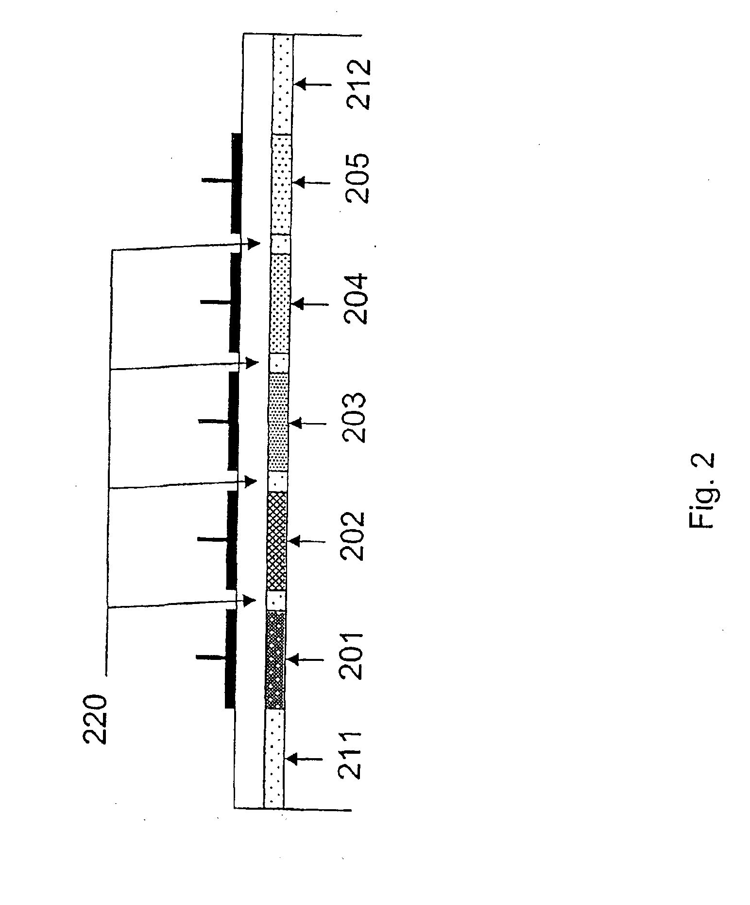
[0034]FIG. 2 shows a cross section through the axial length of the waveguide of the device. The EAM is split into sections 201, 202, 203, 204, 205, each with a different bandgap and in which each bandgap section is addressed by a separate electrode. The device may advantageously have low-loss waveguides 211, 212 at its input and output. Th...


PUM


Abstract

A method of modulating an optical signal passing through a waveguide structure with a plurality of sections including electrically biasing one or more of the sections with a bias voltage to achieve a predetermined level of chirp, modulation depth, or insertion loss. Preferably, two or more sections are biased with a reverse bias voltage, a zero bias voltage, or forward bias voltage.

Description

RELATED APPLICATIONS[0001]This application is a divisional of copending U.S. patent application No. 10 / 507,670 filed Apr. 11, 2005, which is a national stage of International Patent Application No. PCT / GB03 / 01083, filed Mar. 14, 2003 and assigned to the assignee hereof. The specification and drawings of those applications are fully incorporated by reference herein.BACKGROUND OF THE INVENTION[0002]Waveguide electro-absorption modulators (EAMs) are very compact devices suitable for modulating light at data rates of 10 Gb / s and higher. They are used in optical communication networks with a typical reach currently of 50 km, but likely extending to 100 to 120 km in the near future. Optimized devices would have application in even longer reach systems.[0003]Their compact size (typically having a waveguide length of a few hundred μm), low drive voltage (typically <5V) and compatibility with semiconductor lasers in terms of mode size make them ideal for use as external modulators. They c...

Claims


Application Information

Patent Timeline
IPC IPC(8): H01S3/00G02F1/00G02F1/015G02F1/017
CPCB82Y20/00G02F1/01708G02F2201/16G02F2001/0175G02F2001/0157G02F1/0175G02F1/0157
Inventor MARSH, JOHN HAIG
Owner INTENSE LTD
Why Eureka
Try Eureka