Field effect transistor-based biosensor with inorganic film, method of manufacturing the biosensor, and method of detecting biomolecule using the biosensor
- Summary
- Abstract
- Description
- Claims
- Application Information
AI Technical Summary
Benefits of technology
Problems solved by technology
Method used
Image

Examples
example 1
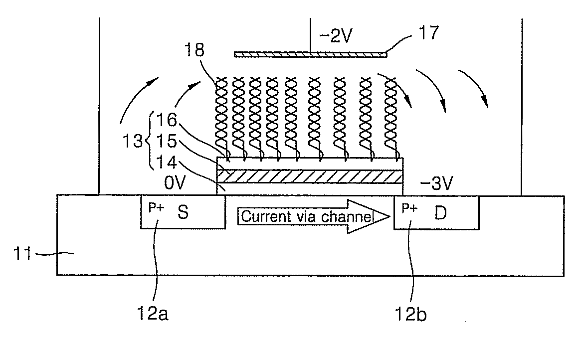
Manufacturing of FET-Based Biosensors According to the Present Invention
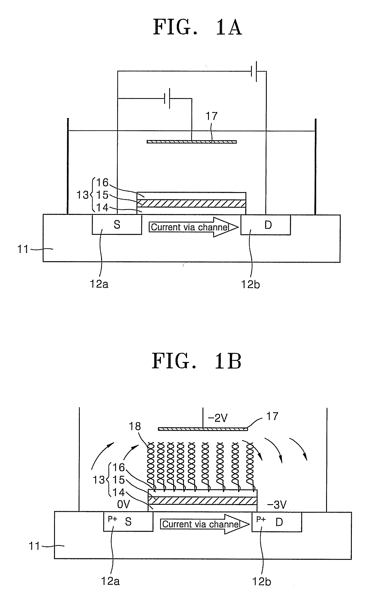
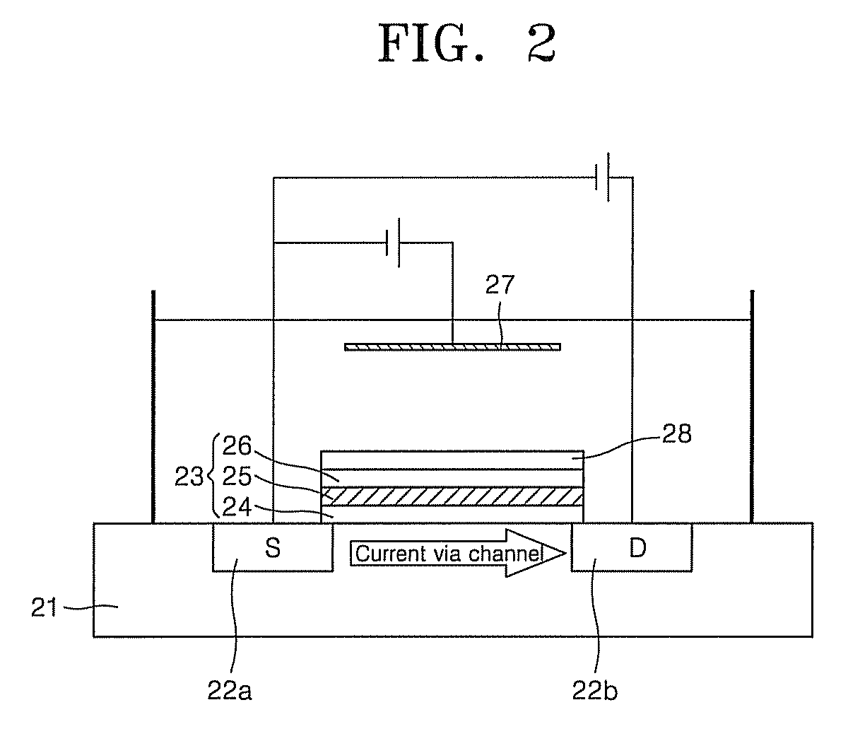
[0053]FET devices were manufactured using an XC10-1.0 um CMOS process in semiconductor fabrication facilities (X-FAB Semiconductor Foundries, Germany). The standard CMOS process differs slightly among manufacturing companies, but these differences do not affect the FET device characteristics and are irrelevant to the present invention. FET-based biosensors according to the invention were manufactured using FET devices as illustrated in the manufacturing method schematically shown in FIG. 3.
[0054]First, the passivation layer of the FET structure was removed, and the gate electrodes were exposed (see (a) of FIG. 3). This process was performed by X-FAB. Then, a surface of the FET structure, including the exposed gate electrodes, was carefully washed and dried. The surface of the FET structure was washed with pure acetone and water using a wet station used in semiconductor fabrication. The FET structure was subseque...
example 2
Manufacturing of FET-Based Biosensors According to the Present Invention
[0057]For this example, the FET-based biosensors were manufactured in the same manner as described in Example 1, except that Al was deposited to a thickness of 20 nm by sputtering, instead of the deposition of Al2O3 by ALD.
[0058]FIG. 4A is an image showing Al deposited on surfaces of gates in the FET-based biosensors manufactured in Example 2, and FIG. 4B is an image showing porous boehmite produced when Al of FIG. 4A is treated with hot water. Referring to FIG. 4B, boehmite was formed to a thickness of 100 nm, and the Al film was mostly converted to the porous boehmite structure.
[0059]For the FET-based biosensor produced according to the procedure described above, the surface resistance of Al was 6.0 MΩ and the surface resistance of boehmite was 0.25 Ω (following treatment with hot water for 5 minutes) and 0.33 MΩ (following treatment with hot water for 30 minutes).
example 3
Detection of Oligonucleotides Using FET-Based Biosensors According to the Present Invention
[0060]The FET-based biosensors manufactured in Example 1 were connected to a parameter analyzer and stabilized. Stabilization of the FET-based biosensors was performed by submerging the FET devices in a 0.1×phosphate buffered saline (PBS) solution while iteratively changing the gate voltage. The gate voltage was then set to 2 V.
[0061]At a predetermined time after the FET devices were stabilized, 25 bp probe oligonucleotides were exposed to the FET-based biosensors. The probe oligonucleotides consisted of a nucleotide sequence of 5′-(GTG TGA GAG TGG AAA GTT CAC ACT G)-3′ (SEQ ID NO: 1), and were used at a concentration of 1 ng / μl. At a predetermined time after the probe oligonucleotides were exposed to the FET-based biosensors, 2 ng / μlμl of PLL was introduced. The oligonucleotides and PLL solutions were each made with 0.01 mM PBS solution (pH 7).
[0062]FIG. 5 is a graph illustrating the change i...
PUM
 Abstract
Description
Claims
Application Information
 - Generate Ideas
- Intellectual Property
- Life Sciences
- Materials
- Tech Scout
- Unparalleled Data Quality
- Higher Quality Content
- 60% Fewer Hallucinations
Browse by: Latest US Patents, China's latest patents, Technical Efficacy Thesaurus, Application Domain, Technology Topic, Popular Technical Reports.
© 2025 PatSnap. All rights reserved.Legal|Privacy policy|Modern Slavery Act Transparency Statement|Sitemap|About US| Contact US: help@patsnap.com