
Micromachined neural probes

a neural probe and micromachine technology, applied in the field of microelectromechanical systems, can solve the problems of not providing much insight into the brain's circuitry at the level of single neurons, and current tools often fall short of providing a densely populated 3-dimensional ‘activity map'

Active Publication Date: 2009-07-09
CALIFORNIA INST OF TECH
View PDF3 Cites 125 Cited by
  • Summary
  • Abstract
  • Description
  • Claims
  • Application Information

AI Technical Summary

Benefits of technology

[0007]In another embodiment, a method of making a neural probe is provided, the method comprising providing a substrate having a thickness of less than 150 μm, such as 100 μm or less; patterning at least one first electro

Problems solved by technology

Techniques such as electroencephalography (EEG) and functional magnetic resonance imaging (fMRI) provide coarse grained views on synchronized activity, but they do not afford much insight into the brain's circuitry at the level of single neurons.
However, current tools often fall short of providing a densely populated 3-dimensional ‘activity map,’ which may offer a better understanding of the circuitry of cell assemblies in the brain.

Method used


Image

  • Micromachined neural probes
  • Micromachined neural probes
  • Micromachined neural probes

Examples


working examples

NON-LIMITING WORKING EXAMPLES

Example 1

Single-Sided Device Process

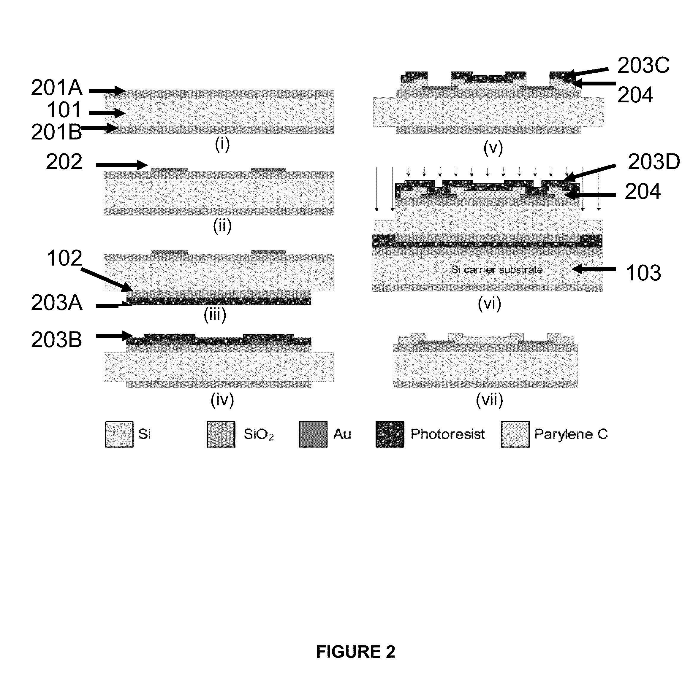
[0053]In some embodiments of this working example, the silicon wafers underwent the handling process as described previously with respect to FIG. 2. The starting material was a double-side polished 2 inch diameter ultra-thin Si (100) substrate with a thickness ranging from 25 μm to 50 μm (Virginia Semiconductor). The substrate was thermally oxidized to yield a oxide layer on both sides. Next, a negative tone photoresist was spun on and patterned to define the recording electrodes, interconnects, and flip-chip contact pads. The metallization was carried out in a thermal evaporator and comprises a 30 Å Cr adhesion layer and a 1500 Å Au layer. The substrate was then ultrasonicated in acetone to lift off the unpatterned metal and photoresist, leaving behind the finished electrode patterns. At this point, the wafer was flipped over, remounted on a temporary carrier, and the oxide was selectively removed on the back side usi...

example 2

Materials and Methods

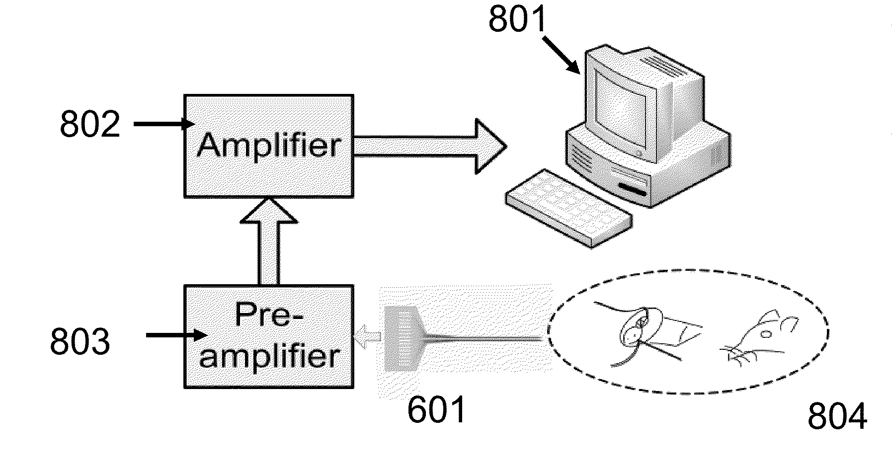
[0061]In this example, a 50 μm thick silicon substrate was patterned on both of its polished surfaces with gold microelectrode arrays. The conducting leads were electrically isolated by a 2 μm plasma-etched parylene C layer deposited over the metal, and 2 μm underlying thermal oxide. The substrate supporting the array was shaped into two sharp shafts by DRIE through the silicon layer. A representative device assembly is shown in FIGS. 15A-15C. In this embodiment, each shaft had dimensions of 4 mm×70 μm×50 μm (l×w×t) and contained eight 100 μm2 electrodes on the front as well as the back side. Shafts were spaced 80 μm apart at their widest point, and electrodes were separated by 25 to 40 μm center-to-center. In order to ensure electrical continuity of the recording sites to off-chip electronics, each structure 601 was flip-chip bonded onto a flexible printed circuit board (PCB) 603 (see FIG. 15C). A modular assembly approach was used to create the multilayer sili...


PUM

PropertyMeasurementUnit
Timeaaaaaaaaaa
Thicknessaaaaaaaaaa
Structureaaaaaaaaaa

Abstract

A neural probe includes at least one shaft, at least one first electrode disposed on a first side of the at least one shaft, and at least one second electrode disposed on a second side of the at least one shaft. The at least one second electrode is separately addressable from the at least first electrode.

Description

CROSS-REFERENCE TO RELATED PATENT APPLICATIONS[0001]This application claims priority to U.S. Provisional Application Ser. No. 61 / 007,990, filed Dec. 17, 2007, incorporated herein by reference in its entirety.BACKGROUND OF THE INVENTION[0002]The invention is related to micro-electro-mechanical systems (MEMS), and specifically to neural probes and methods of making thereof.[0003]There is an increasing demand in neuroscience for large scale recording of neuronal activity (see Buzsáki, G., “Large-scale recording of neuronal ensembles,”Nature Neuroscience, 2004, pp. 446-451, vol. 7). Techniques such as electroencephalography (EEG) and functional magnetic resonance imaging (fMRI) provide coarse grained views on synchronized activity, but they do not afford much insight into the brain's circuitry at the level of single neurons. The introduction of multielectrode silicon probes (see Blanche et al., “Polytrodes: High-density silicon electrode arrays for large-scale multiunit recording,” Jour...

Claims


Application Information

Patent Timeline
IPC IPC(8): A61M37/00A61B5/04
CPCA61B5/04001A61B5/6848A61B2562/028A61N1/0529A61N1/0531Y10T29/49002H01R43/00A61B5/0478A61B5/4839A61M5/00Y10T29/49117A61N1/0551A61B5/4041A61B5/24A61B5/291
Inventor MASMANIDIS, SOTIRIS K.DU, JIANGANGROUKES, MICHAEL L.LAURENT, GILLES J.
Owner CALIFORNIA INST OF TECH
Features
  • Generate Ideas
  • Intellectual Property
  • Life Sciences
  • Materials
  • Tech Scout
  • Unparalleled Data Quality
  • Higher Quality Content
  • 60% Fewer Hallucinations
Learn More