Organic Luminescence Transistor Device and Manufacturing Method Thereof
Inactive Publication Date: 2009-07-16
DAI NIPPON PRINTING CO LTD +2
View PDF2 Cites 22 Cited by
Summary
Abstract
Description
Claims
Application Information
AI Technical Summary
This helps you quickly interpret patents by identifying the three key elements:
Problems solved by technology
Method used
Benefits of technology
Benefits of technology
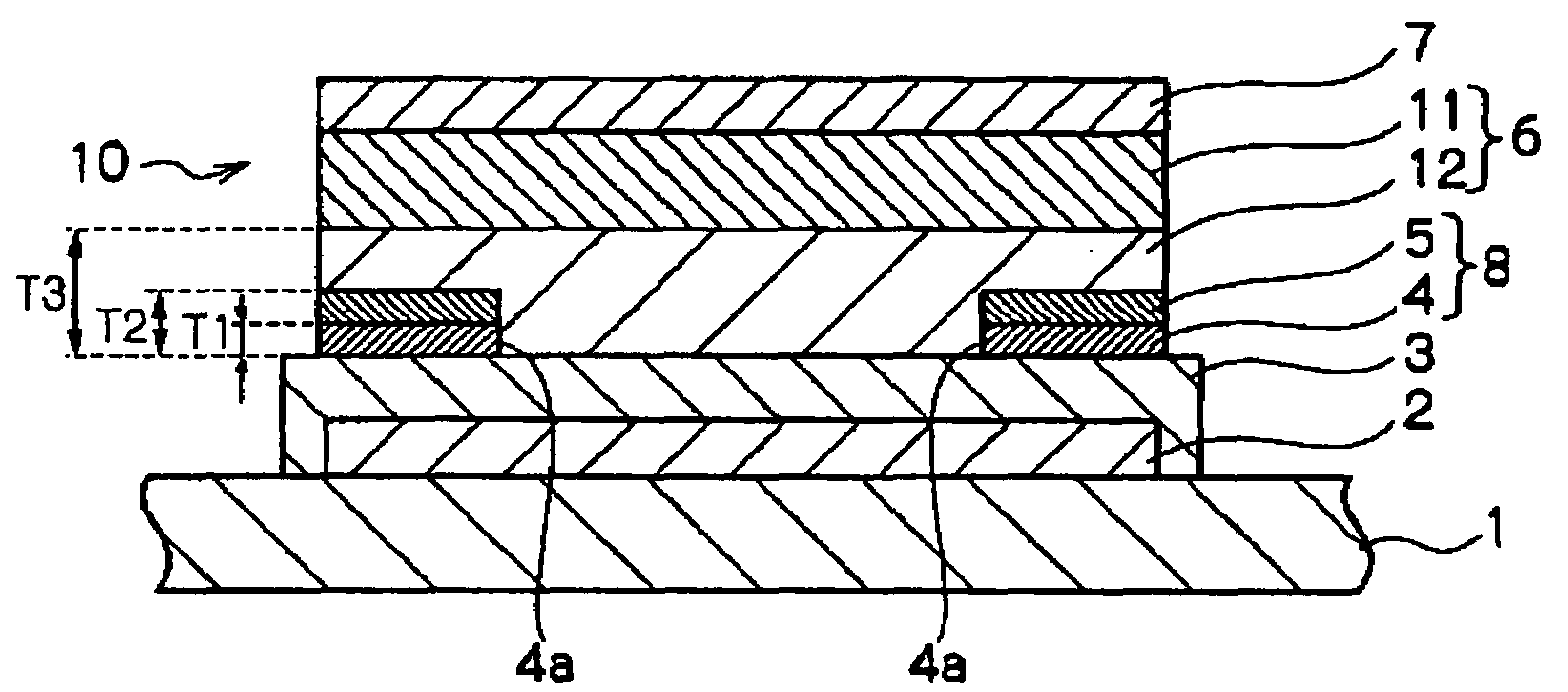
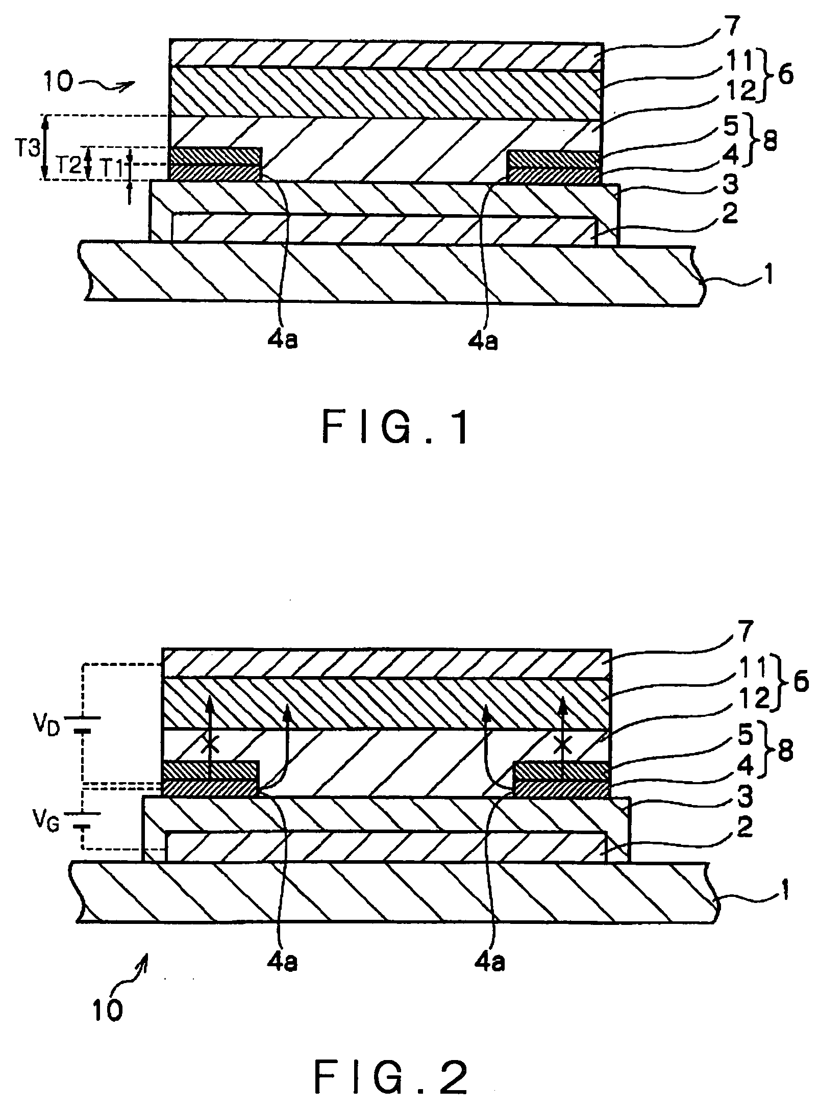
[0010]The present invention is accomplished in order to solve the aforementioned problems. An object of the present invention is to provide a vertical type of organic luminescence transistor device and a manufacturing method thereof wherein a current control between an anode and a cathode is facilitated.
[0029]According to any of the above manufacturing methods of an organic luminescence transistor device, it is possible to form the electric-charge-injection inhibiting layer easily and precisely.
Problems solved by technology
Thus, the amount of the generated electric charges cannot be controlled by controlling the voltage (Vg) to be applied between the assistance electrode 113 and the anode 115, so that it is difficult to control the amount of the luminescence.
Method used
Image
Click on the blue label to locate the original text in one second.
Reading with bidirectional positioning of images and text.
Examples
example 1
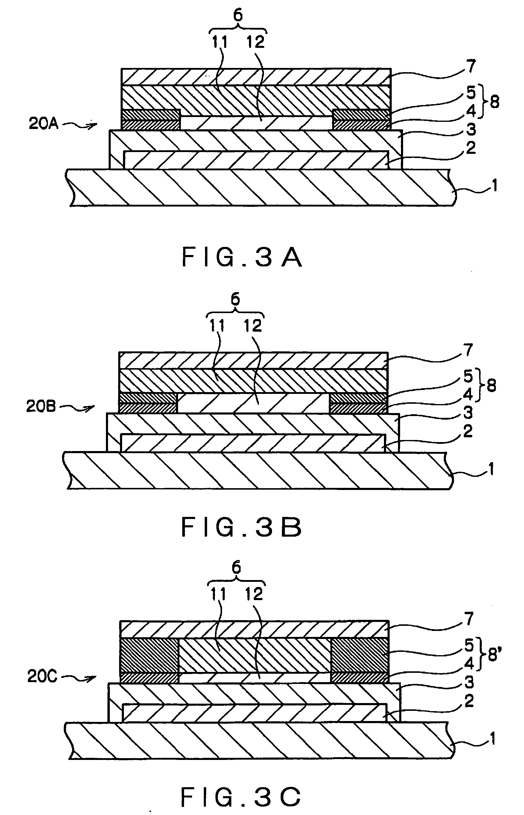
[0132]An insulation film 3 was formed of a PVP-based resist (manufactured by TOKYO OHKA KOGYO CO. Ltd., trade name: TMR-P10), into a 300 nm thickness, by means of a spin coating method, on a glass substrate 1 having an assistance electrode 2 that is made of an ITO film and has a 100 nm thickness.
[0133]Next, by means of a vacuum deposition method using a mask, a first electrode 4 (anode) was formed of Au (whose thickness was 30 nm). Then, in order to cover the first electrode 4, the positive-type resist (manufactured by TOKYO OHKA KOGYO CO. Ltd., trade name: TMR-P10) was applied on the insulation film 3 by means of a spin coating method. Then, an exposing light including wavelengths of 405 nm and 436 nm is irradiated from a side of the substrate 1, so as to expose the positive-type resist film between the first electrodes 4 (anodes) to the light. Then, the positive-type resist film was developed with an alkali development liquid (trade made: NMD-3). Thus, the resist film (whose thick...
example 2
[0137]An insulation film 3 was formed of a PVP-based resist (manufactured by TOKYO OHKA KOGYO CO. Ltd., trade name: TMR-P10), into a 300 nm thickness, by means of a spin coating method, on a glass substrate 1 having an assistance electrode 2 that is made of an ITO film and has a 100 nm thickness.
[0138]Next, by means of a vacuum deposition method using a mask, pentacene (50 nm in thickness) as the electron-charge (positive hole) injection layer 12′ / Au (30 nm in thickness) as the first electrode 4 (anode) / SiO2 (100 nm in thickness) as the electron-charge (positive hole) injection inhibiting layer 5 / pentacene (50 nm in thickness) as the electron-charge (positive hole) injection layer 12 between the laminated structures 8 each of which consists of the first electrode 4 and the electron-charge injection inhibiting layer 5 / α-NPD (90 nm in thickness) as the electric-charge (positive hole) transfer layer 13 / Alq3 (60 nm in thickness) as a luminescent layer 11 / Lif (1 nm in thickness) as an el...
example 3
[0141]An insulation film 3 was formed of a PVP-based resist (manufactured by TOKYO OHKA KOGYO CO. Ltd., trade name: TMR-P10), into a 300 nm thickness, by means of a spin coating method, on a glass substrate 1 having an assistance electrode 2 that is made of an ITO film and has a 100 nm thickness.
[0142]Next, by means of a vacuum deposition method using a mask, a first electrode 4 (anode) was formed of Au (whose thickness was 30 nm). Then, in order to cover the first electrode 4, the positive-type resist (manufactured by TOKYO OHKA KOGYO CO. Ltd., trade name: TMR-P10) was applied on the insulation film 3 by means of a spin coating method. Then, an exposing light including wavelengths of 405 nm and 436 nm is irradiated from a side of the substrate 1, so as to expose the positive-type resist film between the first electrodes 4 (anodes) to the light. Then, the positive-type resist film was developed with an alkali development liquid (trade made: NMD-3). Thus, the resist film (whose thick...
PUM
Abstract
The invention is an organic luminescencetransistor device including: a substrate; an assistance electrode layer provided on an upper surface of the substrate; an insulation film provided on an upper surface of the assistance electrode layer; a first electrode provided locally on an upper surface of the insulation film, the first electrode covering an area of a predetermined size; an electric-charge-injection inhibiting layer provided on an upper surface of the first electrode, the electric-charge-injection inhibiting layer having the same size as the first electrode in a plan view; an electric-charge injection layer provided on the upper surface of the insulation film at an area not provided with the first electrode and on an upper surface of the electric-charge-injection inhibiting layer; a luminescent layer provided on an upper surface of the electric-charge injection layer; and a second electrode layer provided on the luminescent layer.
Description
FIELD OF THE INVENTION[0001]This invention relates to an organic luminescencetransistor device and a manufacturing method thereof. In more details, in a vertical type of organic luminescencetransistor device, this invention relates to an organic luminescence transistor device and a manufacturing method thereof wherein a current control between an anode and a cathode is facilitated.BACKGROUND ART[0002]An organic electroluminescence device has a simple structure, so that it has been expected as a luminescence device for the next generation display that is thinner, lighter, larger area and less costly. Thus, recently, the organic electroluminescence device has been studied hard.[0003]As a driving method for driving the organic electroluminescence device, an active-matrix type of filed effect transistor (FET) that uses a thin film transistor (TFT) is considered to be advantageous in terms of operational speed and power consumption. On the other hand, as a semiconductor material for fo...
Claims
Application Information
Patent Timeline
Application Date:The date an application was filed.
Publication Date:The date a patent or application was officially published.
First Publication Date:The earliest publication date of a patent with the same application number.
Issue Date:Publication date of the patent grant document.
PCT Entry Date:The Entry date of PCT National Phase.
Estimated Expiry Date:The statutory expiry date of a patent right according to the Patent Law, and it is the longest term of protection that the patent right can achieve without the termination of the patent right due to other reasons(Term extension factor has been taken into account ).
Invalid Date:Actual expiry date is based on effective date or publication date of legal transaction data of invalid patent.

