Focus measurement method and method of manufacturing a semiconductor device

a technology of semiconductor devices and manufacturing methods, which is applied in the direction of photomechanical devices, instruments, printers, etc., can solve the problems of shrinkage, affecting the accuracy of focus measurement, so as to achieve accurate focus value and focal shift length, less data, and high accuracy

Active Publication Date: 2009-08-06
PANNOVA SEMIC
View PDF7 Cites 6 Cited by
  • Summary
  • Abstract
  • Description
  • Claims
  • Application Information

AI Technical Summary

Benefits of technology

[0014]The objective of the present invention is to provide a method of enabling accurate and easy focus measurement even in a fine resist pattern whose shrinkage is relatively greater, and a semiconductor manufacturing method using the focus measurement method.
[0017]According to the present invention, even in the fine pattern whose shrinkage becomes relatively great, an accurate focus value and focal shift length can be obtained with lesser data. Then, the focus adjustment per exposure or per unit of exposure (lot) according to the focal shift length enables the inhibition of increase in the focal shift and the formation of a resist pattern with high accuracy. As a result, a semiconductor device can be formed with high production yield.

Problems solved by technology

If an error occurs to a value of the measured length due to this shrinkage, the accuracy of the focus measurement shall worsen by the shrink.
Further, since the resist pattern width itself is small in the manufacturing process generation using the ArF laser lithography, the shrinkage becomes a relatively unignorable size with regard to the dimension of the resist pattern.
In addition, because the shrinkage occurs due to the electron beam irradiation, the pattern shrinks at the same time of the length measurement, and an error shall occur to a value of the measured length.
However, in a fine process with the minimum dimension: 250 nm or less using a chemically-amplified high sensitive resist, particularly in a process requiring fine dimension processing with less than 100 nm, such as 65 nm or 45 nm, there is a concern that the focus measurement becomes more and more difficult due to the shrinkage of the resist film, and the focus measurement suitable for such process is expected.

Method used


Image

  • Focus measurement method and method of manufacturing a semiconductor device
  • Focus measurement method and method of manufacturing a semiconductor device
  • Focus measurement method and method of manufacturing a semiconductor device

Examples


first embodiment

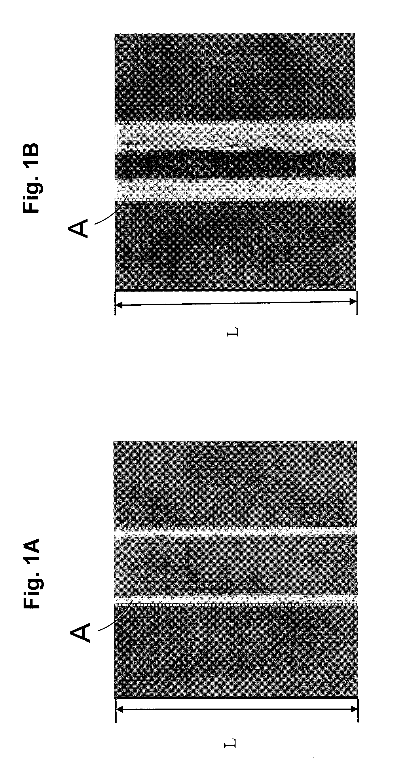
[0030]Hereafter, a first embodiment relating to the present invention will be explained. In the present invention, noticing that a shrinkage by an electron beam is great with a chemically-amplified resist, the shrinkage is digitalized according to the measurement of a resist pattern dimension, and a focus of the exposure apparatus is calculated using the digitalized shrinkage. For the digitalization of the shrinkage, shrinkage of the resist pattern by the electron beam with a CD-SEM (critical dimension-secondary electron microscopy) is utilized. In this embodiment, a dimension measurement point of the resist pattern is fixed and the dimension is repeatedly measured n-times, and the shrinkage occurred by the electron beam irradiation during the measurements is calculated by subtracting the pattern dimension in the n-th measurement from that in the 1 st measurement.

[0031]FIGS. 1A and 1B are SEM image pictures showing a fine resist pattern observed from the upper side with the CD-SEM. ...

second embodiment

[0050]Hereafter, another embodiment regarding an exposure development system using the focus measurement method and the focal shift length calculation method described in the first embodiment, and a photolithography process including a use of this exposure system will be described.

[0051]FIG. 7 is block diagram schematically showing an exposure system in this embodiment. An exposure system 1 performs exposure and development including the focus measurement and the focal shift length calculation process in the lithography process. As shown in FIG. 7, the exposure system 1 is composed of an exposure apparatus 2, a developing apparatus 3, an electron beam length measuring apparatus 4 and a focus measuring apparatus 5. The focus measuring apparatus 5 is composed of a shrinkage calculation unit 6, a focus value calculation unit 7, a focal shift length calculation unit 8, a next-time focus value feedback unit 9 and a memory unit 10. The memory unit 10 stores a database indicating the focal...


PUM

PropertyMeasurementUnit
widthaaaaaaaaaa
wavelengthaaaaaaaaaa
widthaaaaaaaaaa

Abstract

In a focus measurement method and a method of manufacturing a semiconductor device relating to the present invention, a focus value is obtained by using a fluctuation where shrinkage of a resist pattern by an electron beam irradiation depends upon the focus value. In the case of obtaining the focus value, the shrinkage of the resist pattern for a focus measurement formed by exposure to be subject for a focus value measurement is measured. The focus value corresponding to the shrinkage is obtained from the pre-obtained focal dependency of the shrinkage. A focal shift length can be defined from a difference between the focus value and a predetermined best focus value.

Description

CROSS-REFERENCE TO RELATED APPLICATION[0001]The present application claims the benefit of Japanese Patent Application No. 2008-022948 filed Feb. 1, 2008, the subject matter of which is incorporated herein by reference.BACKGROUND OF THE INVENTION[0002]1. Field of the Invention[0003]The present invention mainly relates to a method of measuring and adjusting exposure focus in a lithography process, and a method of manufacturing a semiconductor device using said method.[0004]2. Description of the Related Art[0005]Conventionally, an exposure apparatus (such as, a stepper and the like) is used for forming a fine element pattern of a semiconductor integrated circuit. The exposure apparatus performs projection exposure to form an image of a mask pattern on a reticle to a resist film having photosensitivity formed on a semiconductor substrate. The projected mask pattern is patternized as a pattern of the resist film by developing the exposed resist film. It is necessary to project the mask p...

Claims


Application Information

Patent Timeline
Patent Type & Authority Applications(United States)
IPC IPC(8): G03C5/00G03B27/32
CPCG03F7/70641Y10S430/143
Inventor IDE, RIMIKONODA, KENJIFUKUMOTO, HIROFUMIASAHI, KENICHIUJIMARU, NAOHIKO
Owner PANNOVA SEMIC
Why Eureka
Try Eureka