Manufacturing method of semiconductor device

Active Publication Date: 2009-08-20
HITACHI POWER SEMICON DEVICE
View PDF5 Cites 47 Cited by
  • Summary
  • Abstract
  • Description
  • Claims
  • Application Information

AI Technical Summary

Benefits of technology

[0013]By exposing a substrate to oxygen plasma, a thin film primarily including silicon dioxide is formed on a surface of the substrate. Metal elements existing on a surface of a substrate emerge on the oxidized film, or drawn in the

Problems solved by technology

However, the inventors have found that use of a technique established for silicon is inadequate even in a cleaning technique, and a technique specialized in silicon carbide is necessary.
In particular, it has been found that even if metal contamination removal in the manufacturing method for a silicon semiconductor is applied, as it is, to that for a silicon carbide semiconductor, sufficient effects can not be obtained.
However, if a monocrystalline silicon carbide substrate is dipped into a chemical liquid for oxidizing silicon, the film primarily including silicon dioxide is barely formed, which is different from the case of a silicon substrate.
However, only a special chemical liquid such as a molten potassium hydroxide enables etching of silicon

Method used


Image

  • Manufacturing method of semiconductor device
  • Manufacturing method of semiconductor device
  • Manufacturing method of semiconductor device

Examples


first embodiment

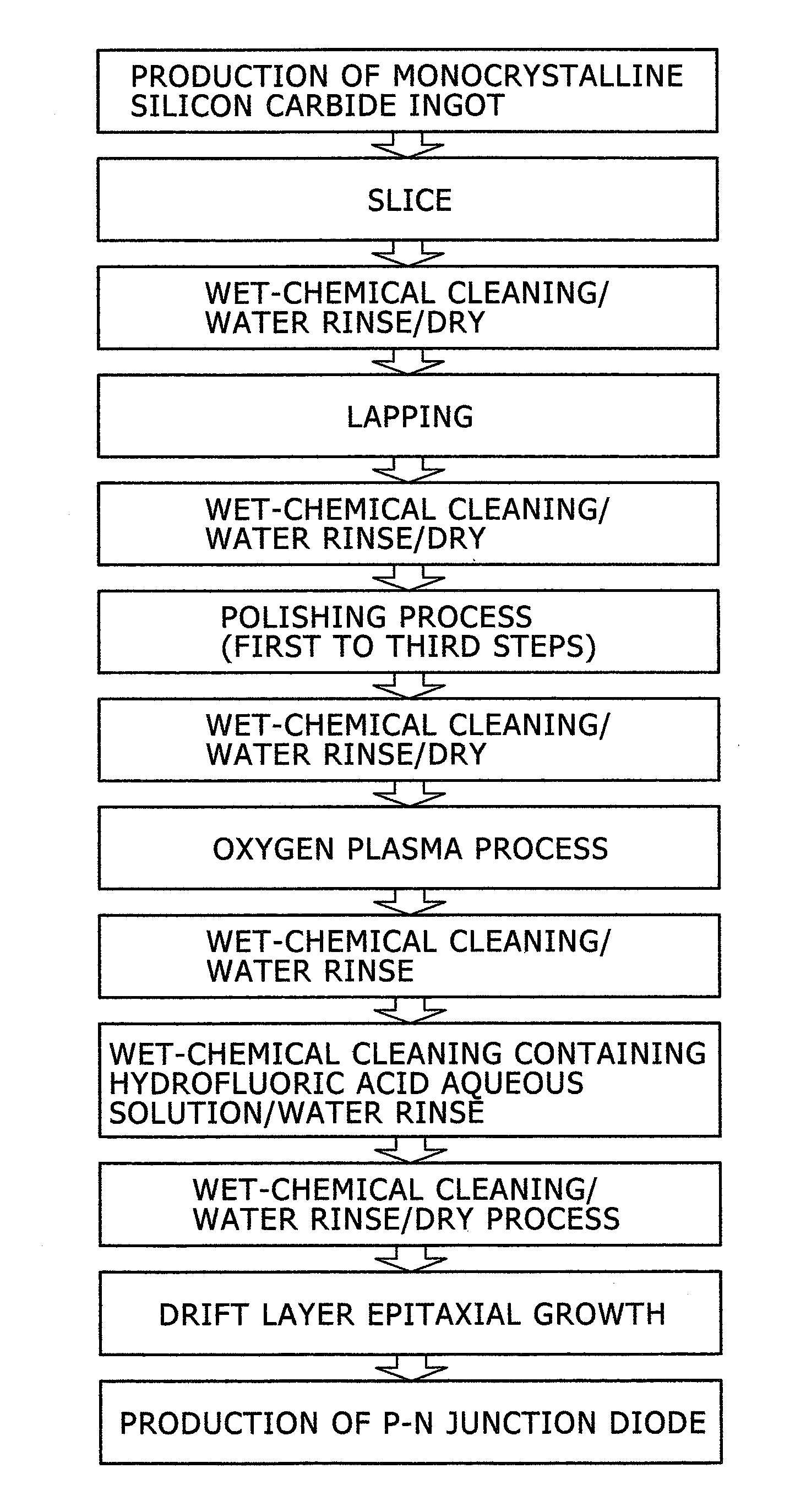
[0071]A first embodiment will be described using FIGS. 1 to 6. The first embodiment is an embodiment applied to manufacturing of a p-n junction diode. In FIG. 1, a process flow of a manufacturing method of a p-n junction diode according to the present invention is shown. In the first place, an ingot made of monocrystalline silicon carbide (4H—SiC) was produced in order to manufacture the monocrystalline silicon carbide substrate. In the manufacturing of the ingot, there was used a sublimation method that is currently the most common method. However, another monocrystalline silicon carbide growth technique such as a dissolution method may be used. As monocrystalline, monocrystalline silicon carbide having other crystal forms such as 2H—SiC, 6H—SiC, and 3C—SiC can be used, in addition to 4H—SiC. 3×1018 cm−3 of nitrogen was contained in monocrystalline silicon carbide of the ingot, and the ingot was of a high-concentration n-type. Next, the produced ingot was sliced to obtain monocryst...

second embodiment

[0088]A second embodiment will be described using FIGS. 6 to 10. The second embodiment is an embodiment applied to manufacturing of a p-n junction diode. A 4H—SiC, 4° off monocrystalline silicon carbide substrate used in the second embodiment was purchased from a manufacturer of a substrate with designated specification. The front surface of the crystal substrate is a silicon plane ((0001) plane), and the back surface thereof is a carbon plane ((000-1) plane). The front surface has a (0001) plane with 4° off-angle inclined toward [11-20]. The epitaxial growth of the drift layer on the substrate was also carried out by the manufacturer of a substrate. After inspection of the delivered substrate, it was found that the diameter was 76.2 mm at the most, and primary and secondary orientation flats were formed. The thickness thereof was 350 μm.

[0089]The concentration of nitrogen of the epitaxial layer was 2×1016 cm−3 and the thickness thereof was 8 μm, which were as designated specificati...

third embodiment

[0097]A third embodiment will be described using FIGS. 11A to 11G. The third embodiment is an embodiment in which the present invention was applied to manufacturing of a JBS diode formed by combining a Schottky barrier and a p-n junction. FIGS. 11A to 11C are cross sectional views each showing a manufacturing process of the JBS diode of the third embodiment. A termination area for relaxing the electric field was formed around the JBS diode, but the illustration thereof was omitted in FIGS. 11A to 11F. As shown in FIG. 11C, the JBS diode of the third embodiment includes an n-type drift layer 112 containing nitrogen which is provided on a front surface of a monocrystalline silicon carbide substrate 111 and has a thickness of about 20 μm, a p-type doped layer 113 containing Al which is provided on a part of a surface of the drift layer 112 and has a thickness of 1 μm, and a high-concentration p-type layer 114 containing Al which is provided on the upper side of the p-type doped layer 1...


PUM


Abstract

A problem in the conventional technique is that metal contamination on a silicon carbide surface is not sufficiently removed in a manufacturing method of a semiconductor device using a monocrystalline silicon carbide substrate. Accordingly, there is a high possibility that the initial characteristics of a manufactured silicon carbide semiconductor device are deteriorated and the yield rate is decreased. Further, it is conceivable that the metal contamination has an adverse affect even on the long-term reliability of a semiconductor device. In a manufacturing method of a semiconductor device using a monocrystalline silicon carbide substrate, there is applied a metal contamination removal process, on a silicon carbide surface, including a step of oxidizing the silicon carbide surface and a step of removing a film primarily including silicon dioxide formed on the silicon carbide surface by the step.

Description

CLAIM OF PRIORITY[0001]The present application claims priority from Japanese patent application JP 2008-034699 filed on Feb. 15, 2008, the content of which is hereby incorporated by reference into this application.BACKGROUND OF THE INVENTION [0002]1. Field of the Invention[0003]The present invention relates to a manufacturing method of a semiconductor device using a monocrystalline silicon carbide substrate.[0004]2. Description of the Related Arts[0005]A conventional power semiconductor device (power semiconductor device) has been manufactured by using a monocrystalline silicon substrate. The progress of design and manufacturing techniques of elements has reduced resistance (on-resistance) at the time of applying current while keeping a high breakdown voltage to realize low loss. However, the breakdown voltage and on-resistance have a trade-off relation in which they are determined on the basis of a band gap of the material of a substrate, and thus, there is a limit to improvement o...

Claims


Application Information

Patent Timeline
IPC IPC(8): H01L21/46
CPCH01L29/1608H01L29/41766H01L29/45H01L29/513H01L29/6606H01L21/02378H01L29/7813H01L29/7828H01L29/8611H01L29/872H01L29/66068
Inventor YOKOYAMA, NATSUKISOMEYA, TOMOYUKI
Owner HITACHI POWER SEMICON DEVICE
Why Eureka
Try Eureka