Magnetic Induction Grid as an Early Warning Mechanism for Space Based Microelectronics

a microelectronics and induction grid technology, applied in the direction of emergency protective arrangements for limiting excess voltage/current, electrical equipment, and arrangements responsive to excess current, can solve the problems of single event effect, signal spike, noise, and microelectronic devices operating, and achieve the effect of preventing single event effect, reducing noise, and reducing nois

Inactive Publication Date: 2009-09-17
IBM CORP
View PDF10 Cites 11 Cited by
  • Summary
  • Abstract
  • Description
  • Claims
  • Application Information

AI Technical Summary

Benefits of technology

[0011]The disadvantages of the prior art are overcome by the present invention which, in one aspect, is a system for protecting an electronic device from cosmic rays that includes a frame in which the circuit is disposed, a cosmic ray detection circuit and a protection circuit. The cosmic ray detection circuit is supported by the frame and is spaced apar

Problems solved by technology

Microelectronic devices operated in space and high altitudes are typically subjected to a barrage of charged particles that often strip electrons or the create electron/hole pairs.
Such interference can result in signal spikes, noise, and single-effect events (SEE).
This ionization may cause a highly localized effect such as a benign glitch in output, a less benign bit flip in memory or a register, or (especially in high-power transistors) a destructive latch-up and burnout.
Single event effects can be disruptive in satellites, aircraft, and other aerospace applications (both civilian and military).
However, in very sensitive devices a single ion can cause a multiple-bit upset (MBU) in several adjacent memory cells.
SEUs can result in single-event functional interrupts (SEFI) when they cause a device to enter into an undefined state, a test mode, or a halt, each of which require a reset or a power cycle for a recovery.
As the effect occurs between the power source and the substrate, destructively high current can be involved and the part may fail.
Bulk CMOS devices are most susceptible to this type of SEE.
When an ion hits near the drain junction, it can cause avalanche multiplication of the charge c

Method used


Image

  • Magnetic Induction Grid as an Early Warning Mechanism for Space Based Microelectronics
  • Magnetic Induction Grid as an Early Warning Mechanism for Space Based Microelectronics
  • Magnetic Induction Grid as an Early Warning Mechanism for Space Based Microelectronics

Examples


Embodiment Construction

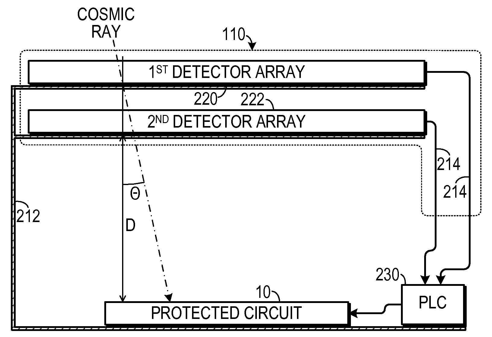
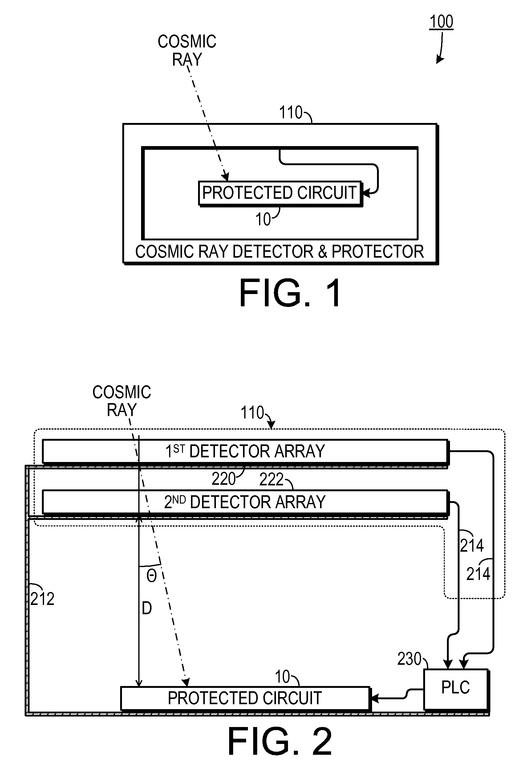
[0021]A preferred embodiment of the invention is now described in detail. Referring to the drawings, like numbers indicate like parts throughout the views. As used in the description herein and throughout the claims, the following terms take the meanings explicitly associated herein, unless the context clearly dictates otherwise: the meaning of “a,”“an,” and “the” includes plural reference, the meaning of “in” includes “in” and “on.” Also, as used herein “cosmic ray” includes any electromagnetic interference in motion (including a charged particle) that is capable of interfering with the operation of an electronic circuit.

[0022]As shown in FIG. 1, one embodiment of an electronic system 100 suitable for exposure to a cosmic ray environment includes an electronic device 10, such as a microelectronic circuit. A cosmic ray detector and protection circuit 110 detects an incoming cosmic ray and causes the electronic system to take protective action when a cosmic ray is detected.
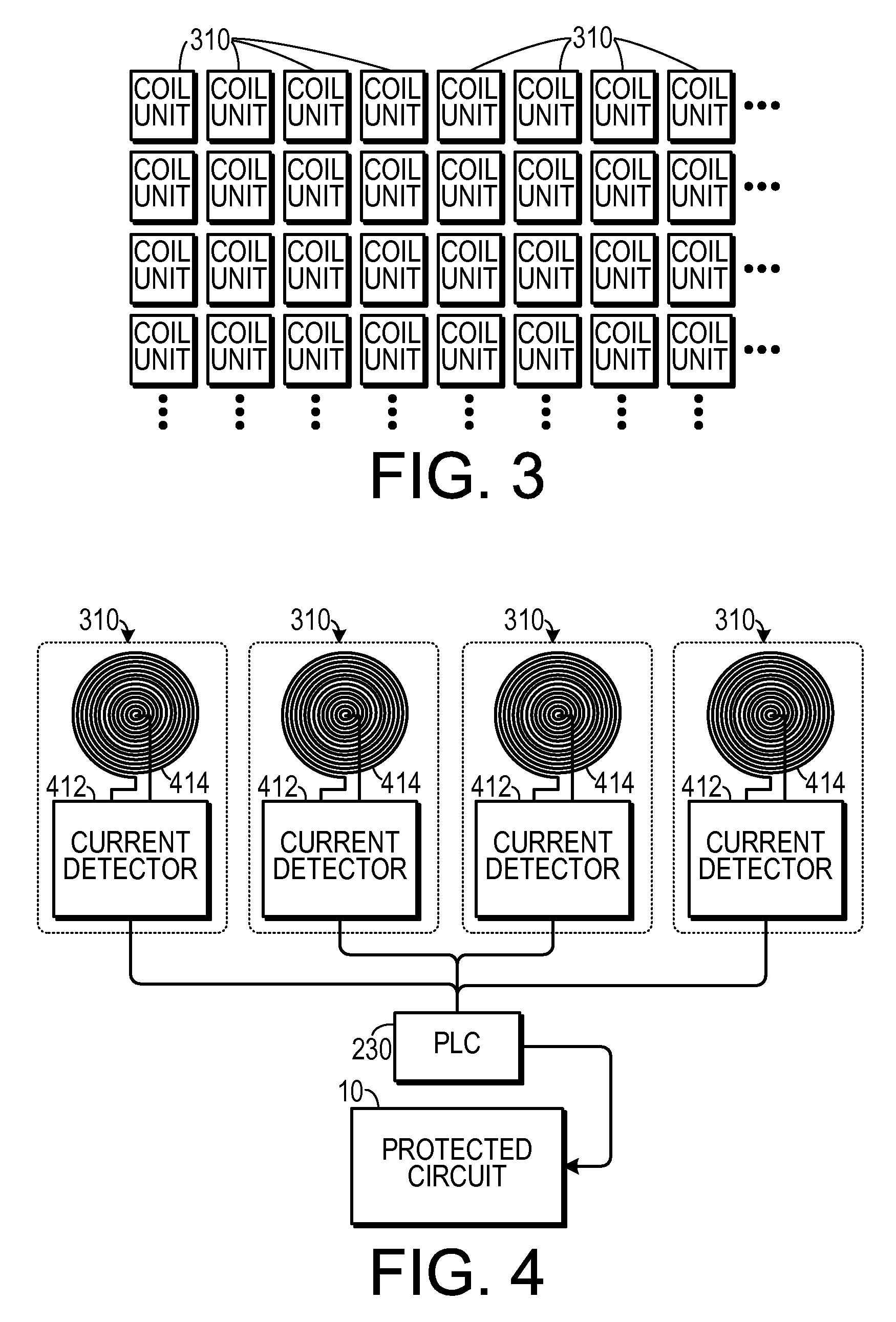
[0023]One ...


PUM


Abstract

A system for protecting an electronic device from cosmic rays includes a frame in which the circuit is disposed, a cosmic ray detection circuit and a protection circuit. The cosmic ray detection circuit is supported by the frame and is spaced apart from the circuit. The cosmic ray detection circuit is configured to assert an incoming cosmic ray signal when a cosmic ray interacts with the cosmic ray detection device. The protection circuit is coupled to the incoming cosmic ray signal and is configured to cause the electronic device to enter a protected state when the cosmic ray signal is asserted.

Description

BACKGROUND OF THE INVENTION[0001]1. Field of the Invention[0002]The present invention relates to error prevention devices and, more specifically, to a device that prevents errors due to cosmic rays.[0003]2. Description of the Prior Art[0004]Microelectronic devices operated in space and high altitudes are typically subjected to a barrage of charged particles that often strip electrons or the create electron / hole pairs. Such interference can result in signal spikes, noise, and single-effect events (SEE). SEEs can have a significant impact on digital devices.[0005]When a high-energy particle travels through a semiconductor, it leaves an ionized track behind. This ionization may cause a highly localized effect such as a benign glitch in output, a less benign bit flip in memory or a register, or (especially in high-power transistors) a destructive latch-up and burnout. Single event effects can be disruptive in satellites, aircraft, and other aerospace applications (both civilian and mili...

Claims


Application Information

Patent Timeline
IPC IPC(8): H02H9/02
CPCH02H5/005
Inventor BRANSFORD, MARK A.MANDELMAN, JACK A.
Owner IBM CORP
Why Eureka
Try Eureka