Semiconductor device and method for manufacturing the same

Inactive Publication Date: 2009-10-22
SEMICON ENERGY LAB CO LTD
View PDF30 Cites 194 Cited by
  • Summary
  • Abstract
  • Description
  • Claims
  • Application Information

AI Technical Summary

Benefits of technology

[0011]An object of one embodiment of the present invention is to provide a semiconductor device in which a glass substrate is used as a base substrate and the S value of a transistor including a single crystal semiconductor film formed by an ion introduction separation method is small, and a method for manufacturing the semiconductor device. Further, another obj

Problems solved by technology

In the case of forming a single crystal semiconductor film by an ion introduction separation method, defects increase in the single crystal semiconductor film by the ion introduction.
In the case where a large number of defects exist in the single crystal semiconductor film, a defect level is likely to be formed at an interface with a gate insulating film.
Accordingly, characteristics of a semiconductor element

Method used


Image

  • Semiconductor device and method for manufacturing the same
  • Semiconductor device and method for manufacturing the same
  • Semiconductor device and method for manufacturing the same

Examples


Example

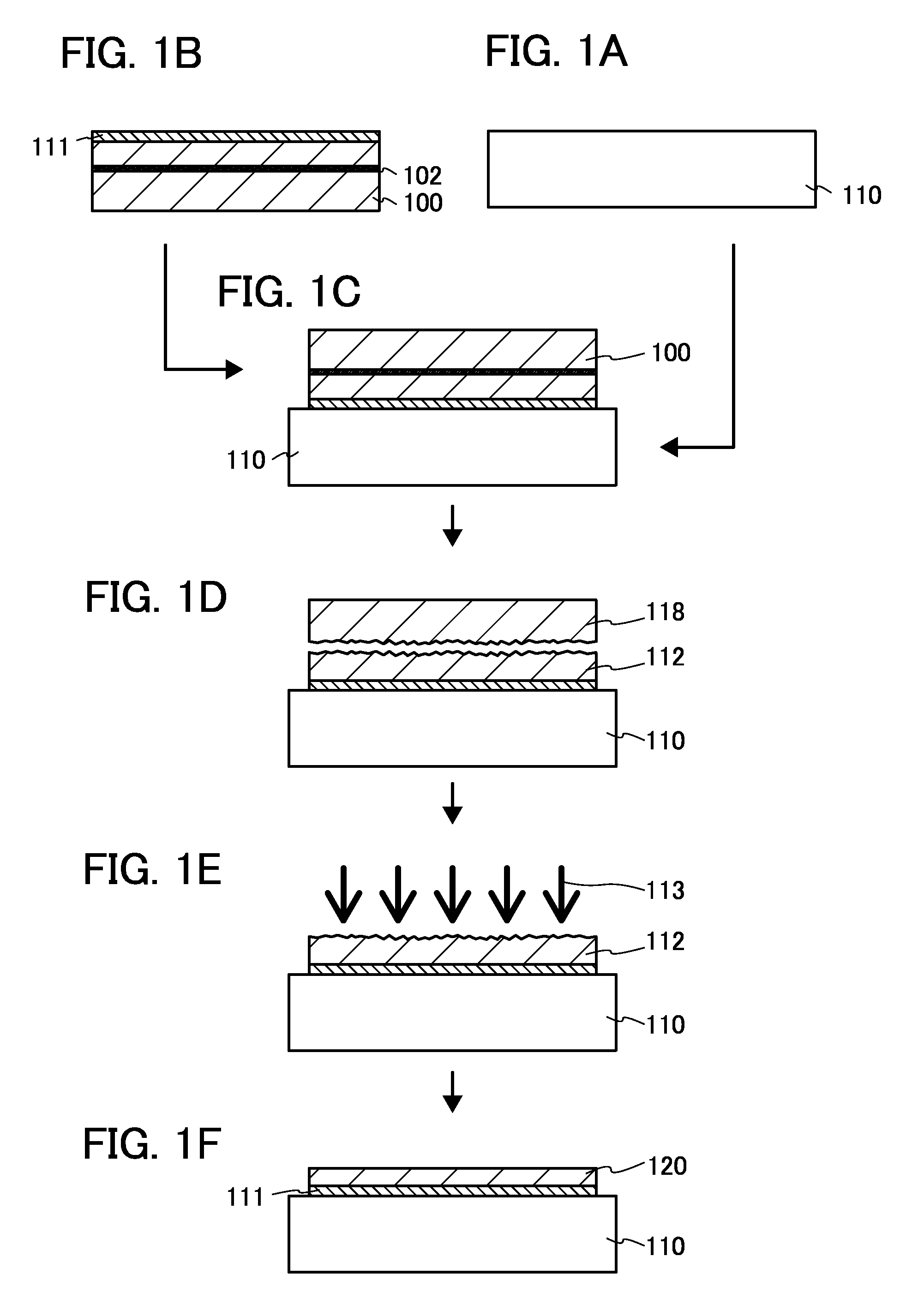
[0031]In Embodiment 1, a manufacturing method of a semiconductor device according to an embodiment of the present invention will be described with reference to FIGS. 1A to 1F, FIGS. 2A to 2D, FIGS. 3A to 3D, and FIGS. 4A and 4B.

[0032]First, a base substrate (also referred to as a supporting substrate) 110 is prepared (see FIG. 1A). As the base substrate 110, a light-transmitting glass substrate used for liquid crystal display devices or the like can preferably be used. As a glass substrate, a substrate having a strain point of higher than or equal to 580° C. and lower than or equal to 680° C. (preferably, higher than or equal to 600° C. and lower than or equal to 680° C.) may be used. Further, it is preferable that the glass substrate be a non-alkali glass substrate. As a material of the non-alkali glass substrate, a glass material such as aluminosilicate glass, aluminoborosilicate glass, or barium borosilicate glass is used, for example.

[0033]Note that as the base substrate 110, a ...

Example

Embodiment 2

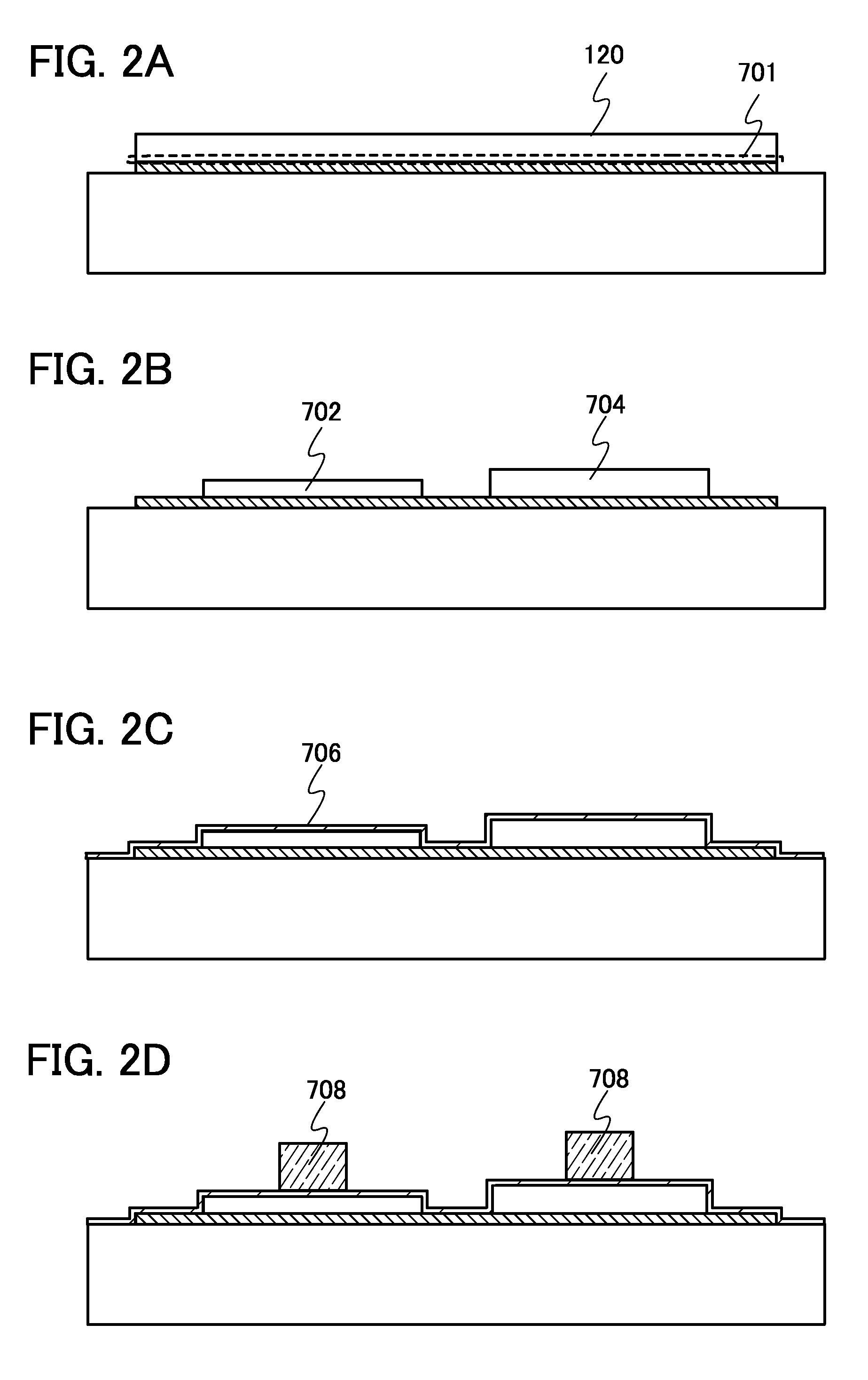
[0102]In Embodiment 2, a preferable thickness of a single crystal semiconductor layer in a transistor which is a semiconductor device of the present invention as manufactured in Embodiment 1, will be described with reference to FIG. 5, FIG. 6, FIGS. 7A and 7B, FIGS. 8A and 8B, FIGS. 9A to 9C, and FIGS. 10A to 10F.

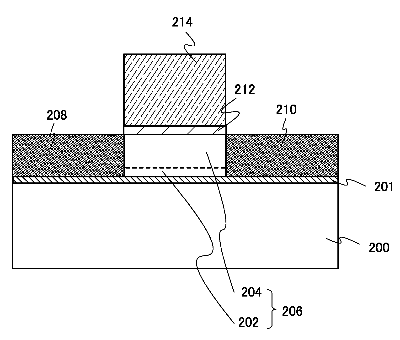
[0103]FIG. 5 illustrates a cross section of the transistor manufactured in Embodiment 1, which is used for evaluating transistor characteristics in this embodiment. Here, the transistor has a single-drain structure in which sidewalls 714, a pair of low-concentration impurity regions 718, and a pair of low-concentration impurity regions 724 are not formed.

[0104]The transistor of FIG. 5 includes a base insulating layer 201 formed over a base substrate 200, a single crystal semiconductor layer 206 formed over the base insulating layer 201, a gate insulating film 212 formed over the single crystal semiconductor layer 206, and a gate electrode 214 formed over the gat...

Example

Embodiment 3

[0118]A semiconductor device such as a transistor is manufactured using a semiconductor substrate according to the present invention, and a variety of electronic devices can be manufactured using this semiconductor device. Since crystal defects in the single crystal semiconductor layer provided for the semiconductor substrate according to the present invention are reduced, the local state density at an interface with a gate insulating layer can be reduced. By using this single crystal semiconductor layer as an active layer, leakage current is reduced; accordingly, a semiconductor element with improved electric characteristics can be manufactured. That is, by using a semiconductor substrate according to the present invention, a semiconductor element with high current driving capability and high reliability can be manufactured; accordingly, an electronic device as a final product can be manufactured with high throughput and favorable quality. In this embodiment, examples o...


PUM


Abstract

A single crystal semiconductor substrate including an embrittlement layer is attached to a base substrate with an insulating layer interposed therebetween, and the single crystal semiconductor layer is separated at the embrittlement layer by heat treatment; accordingly, a single crystal semiconductor layer is fixed over the base substrate. The single crystal semiconductor layer is irradiated with a laser beam so that the single crystal semiconductor layer is partially melted and then is re-single crystallized, whereby crystal defects are removed. In addition, an island-shaped single crystal semiconductor layer for forming an n-channel transistor is channel-doped using a photomask and then is etched back using the photomask so that the island-shaped single crystal semiconductor layer for forming an n-channel transistor is thinner than the island-shaped single crystal semiconductor layer for forming a p-channel transistor.

Description

BACKGROUND OF THE INVENTION[0001]1. Field of the Invention[0002]The present invention relates to semiconductor devices and methods for manufacturing the semiconductor devices. The present invention particularly relates to a semiconductor device which uses a single crystal semiconductor film formed by a hydrogen ion introduction separation method and a method for manufacturing the same.[0003]2. Description of the Related Art[0004]In recent years, integrated circuits using a silicon-on-insulator (SOI) substrate where a thin single crystal semiconductor film is present over an insulating surface, instead of using a bulk silicon wafer, have been developed. By utilizing characteristics of a thin single crystal silicon layer formed over an insulating film, transistors formed in the integrated circuit can be separated from each other completely. Further, since fully-depleted transistors can be formed, a semiconductor integrated circuit with high added value such as high integration, high s...

Claims


Application Information

Patent Timeline
IPC IPC(8): H01L21/336
CPCH01L21/76254H01L29/78621H01L27/1233H01L21/84
Inventor OHNUMA, HIDETONOMURA, NORITSUGU
Owner SEMICON ENERGY LAB CO LTD
Why Eureka
Try Eureka