Semiconductor exposure device using extreme ultra violet radiation

a technology of ultra violet radiation and exposure device, which is applied in the field of exposure device of semiconductor, can solve the problems of reducing the transmission efficiency of euv radiation, superimposing a total of 2000, and low reliability and convenience of use, and achieves the effect of enhancing the purity of extreme ultra violet radiation and high purity

Active Publication Date: 2009-10-29
GIGAPHOTON
View PDF17 Cites 34 Cited by
  • Summary
  • Abstract
  • Description
  • Claims
  • Application Information

AI Technical Summary

Benefits of technology

[0019]The present invention has been conceived in view of the problems described above, and an objective thereof is to provide a semiconductor exposure device, which can irradiate extreme ultra violet radiation of high purity upon a mask. Another objective of the present invention is to provide such a semiconductor exposure device, which, by using a mirror which is made by laminating together a plurality of regions in which the numbers and shapes of the multi layers are different, makes it possible to enhance the purity of the extreme ultra violet radiation by utilizing beneficial diffraction effects of several types. Yet further objectives of the present invention will become clear from the subsequent description of certain embodiments thereof.

Problems solved by technology

The second problem is that, with the prior art technique described above in which the multi layer is subjected to blazing processing, it is necessary to superimpose a total of 2000 or more of the Mo / Si multi layers.
Moreover, if a thin layer film type SPF is used, the transmission efficiency for EUV radiation is decreased, since the transmittivity for EUV radiation is low.
Moreover, in the case of such a thin layer film type SPF, there is a possibility of deformation or damage due to the absorption of infrared radiation and the like, and accordingly the reliability and the convenience of use are low.

Method used


Image

  • Semiconductor exposure device using extreme ultra violet radiation
  • Semiconductor exposure device using extreme ultra violet radiation
  • Semiconductor exposure device using extreme ultra violet radiation

Examples


embodiment 1

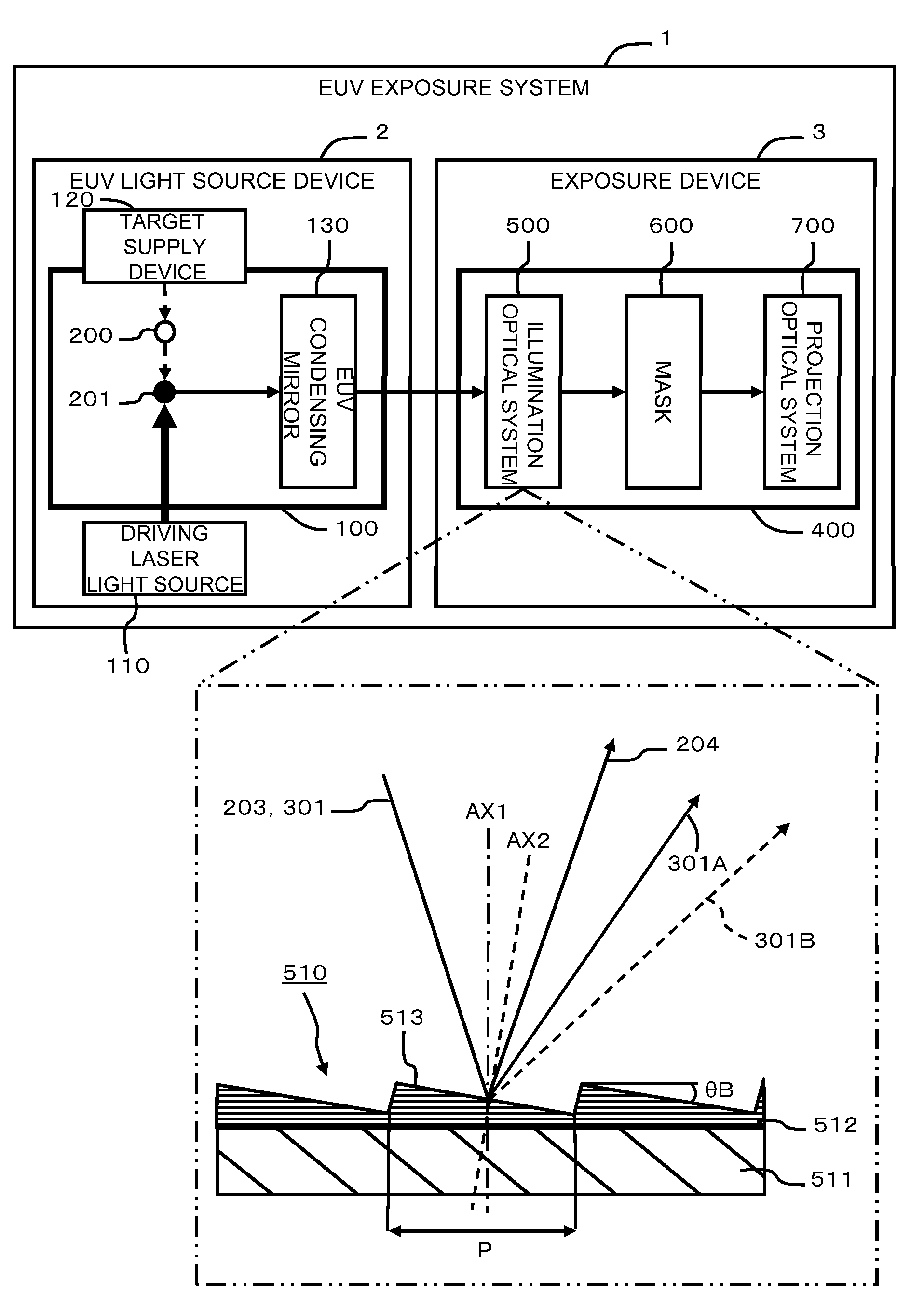
[0056]A first embodiment will now be explained with reference to FIGS. 1 through 10. FIG. 1 is an explanatory figure, schematically showing the overall structure of an EUV exposure system 1. This exposure system 1, for example, comprises an EUV light source device 2 and an exposure device 3.

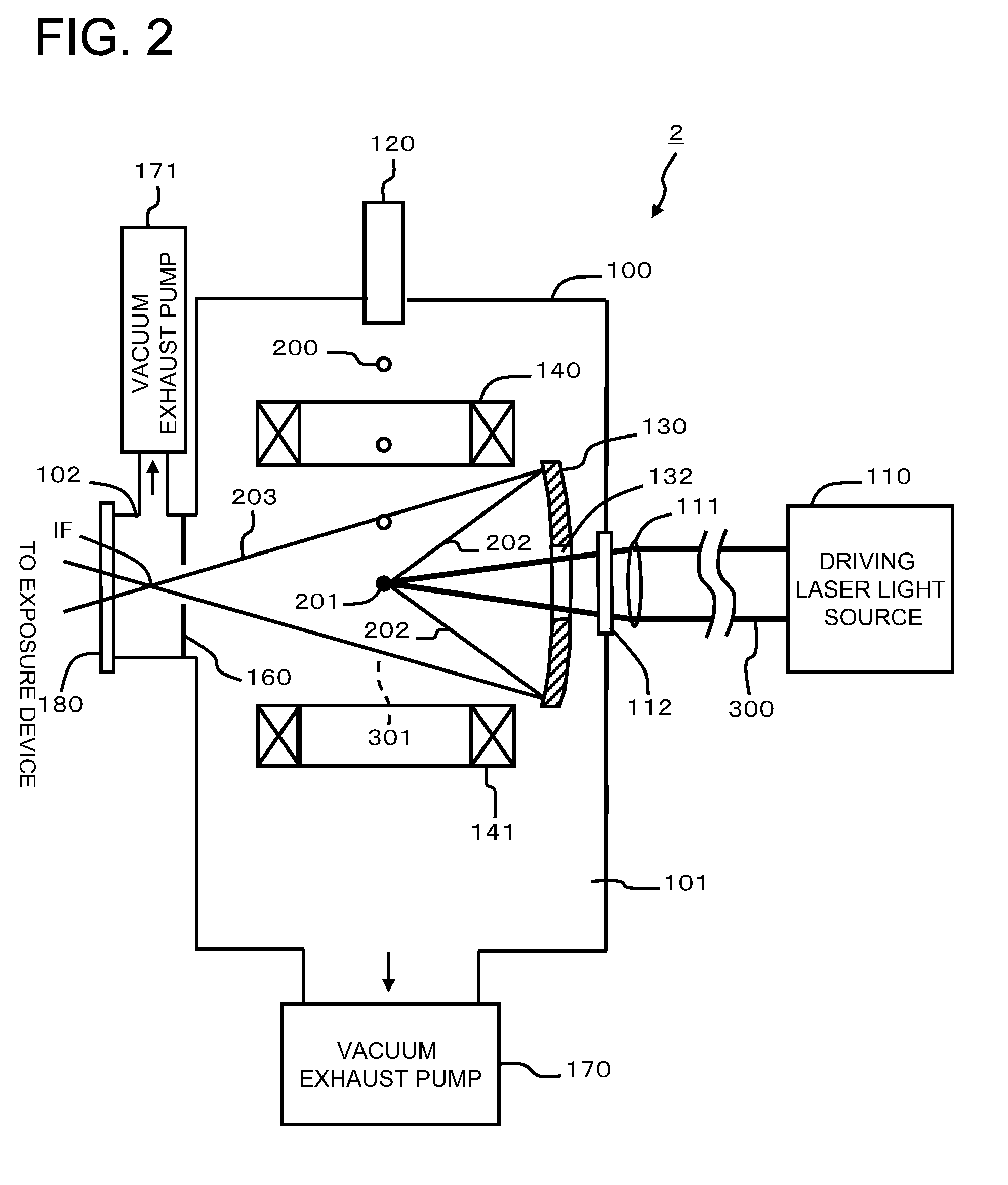
[0057]The details of the EUV light source device 2 will be described in more detail subsequently, but now a first summary will be given. The EUV light source device 2 is a device which generates EUV radiation and supplies it to the exposure device 3. A target supply device 120 supplies a target 200 made from tin or the like into a vacuum chamber 100. A driver laser light source 110 irradiates a driver laser upon the target 200 and converts it into plasma 201. The EUV radiation which is generated from this plasma 201 is collected by an EUV collector mirror 130 and is conducted towards the exposure device 3.

[0058]The exposure device 3 comprises, for example, an illumination optical system 500, a ma...

embodiment 2

[0117]A second embodiment of the present invention will now be explained on the basis of FIGS. 11 through 13. The various embodiments of the present invention which are described below correspond to variants of the first embodiment described above. Accordingly, the explanation thereof will focus upon the aspects in which these embodiments differ from the first embodiment. The aspects of difference between this second embodiment and the first embodiment are that the blazed grooves are formed as concentric circles, that the blazed grooves are formed so that their abrupt step portions face away from the center of the mirror (its central axis) towards the outer edge of the mirror and their gently sloping portions face towards the central axis of the mirror, i.e. so that the blazed grooves are angled in the opposite direction to those of the first embodiment described above, and that, along with this point of difference, a dumper 560 is additionally provided.

[0118]FIG. 11 is an explanato...

embodiment 3

[0124]A third embodiment will now be explained on the basis of FIG. 14. FIG. 14 is an explanatory figure showing the structure of an exposure device 3B according to this embodiment. In this embodiment, blazed grooves are formed upon an inlet mirror 570 upon which the radiation from the EUV light source device 2 is initially incident. The collimator mirror 510B of this embodiment is different from the collimator mirrors 510 and 510A of the embodiments described above, in that no blazed grooves are provided thereupon. In other words, the collector mirror 510B of this embodiment is a mirror which simply reflects radiation which is incident onto it into parallel radiation, but is not endowed with the function of operating as an SPF.

[0125]A plurality of parallel blazed grooves are formed upon the inlet mirror 570, just as was the case with the collimator mirror 510 described with reference to the first embodiment. In other words, the inlet mirror 570 is made by laminating 300 pair layers...


PUM


Abstract

The exposure device is able to supply only EUV radiation to a mask, while eliminating radiation other than the EUV radiation. A multi layer made from a plurality of Mo / Si pair layers is provided upon the front surface of a mirror, and blazed grooves are formed in this multi layer. Radiation which is incident from a light source device is incident upon this mirror, and is reflected or diffracted. Since the reflected EUV radiation (including diffracted EUV radiation) and the radiation of other wavelengths are reflected or diffracted at different angles, accordingly their directions of progression are different. By eliminating the radiation of other wavelengths with an aperture and / or a dumper, it is possible to irradiate a mask only with EUV radiation of high purity.

Description

BACKGROUND OF THE INVENTIONTechnical Field[0001]The present invention relates to a semiconductor exposure device which uses extreme ultra violet radiation.[0002]For example, a semiconductor chip may be created by projecting a mask upon which a circuit pattern is drawn, in reduced form, upon a wafer to which a resist has been applied, and by repeatedly performing processing such as etching and thin layer formation and so on. Along with the progressive reduction of the scale of semiconductor processing, the use of radiation of progressively shorter and shorter wavelengths is required.[0003]Thus, research is being performed into a semiconductor exposure technique which uses radiation of extremely short wavelength, such as 13.5 nm, and a reducing optical system. This type of technique is termed EUV-L (Extreme Ultra Violet Lithography: exposure using extreme ultra violet radiation). Hereinafter, extreme ultraviolet will be abbreviated as “EUV”. An EUV exposure system which uses EUV radia...

Claims


Application Information

Patent Timeline
Patent Type & Authority Applications(United States)
IPC IPC(8): G21K5/00
CPCB82Y10/00G03F7/70575G21K1/062H05G2/003G21K2201/064G21K2201/067G21K2201/061
Inventor MORIYA, MASATOWAKABAYASHI, OSAMUSOUMAGNE, GEORG
Owner GIGAPHOTON
Why Eureka
Try Eureka