Nonvolatile semiconductor memory apparatus

a semiconductor memory and non-volatile technology, applied in the direction of electrical equipment, semiconductor devices, basic electric elements, etc., can solve the problems of adverse effects on the reliability of the tunnel insulating film, unsuitable, and high voltage, and achieve the effect of restricting the leakage current and increasing the leakage curren

Active Publication Date: 2009-10-29
KIOXIA CORP
View PDF6 Cites 11 Cited by
  • Summary
  • Abstract
  • Description
  • Claims
  • Application Information

AI Technical Summary

Benefits of technology

[0017]The present invention has been made in view of these circumstances, and an object thereof is to provide a nonvolatile semiconductor memory apparatus having a tunnel in

Problems solved by technology

However, a higher electric field Eox leads to a higher voltage, which is not desirable.
If the voltage becomes higher, the reliability of the tunnel insulating film is adversely affected.
It is considered that this phenomenon is caused by defects formed in the tunnel insulating film.
The holes generated here travel in the direction opposite to the traveling direction of the electrons, and cause defects in the tunnel insulating film.
However, if the tunnel insulating film becomes 5 nm or less, the D-T (Direct Tunneling) current becomes dominant even when the electric field Eox is a low electric field of 3 MV/cm, and the requirements of the tunnel insulating film are not satisfied.
Therefore, the film thickness of a tunnel insulating film having a trapping level cannot be reduced to 5 nm or less.
However, such a tunnel insulating film having a trapping level is disadvantageous in that its film thickness cannot be made 5 nm or less, since the charge retention properties as a nonvolatile semiconductor memory apparatus are degraded if the leakage current becomes higher i

Method used


Image

  • Nonvolatile semiconductor memory apparatus
  • Nonvolatile semiconductor memory apparatus
  • Nonvolatile semiconductor memory apparatus

Examples


first embodiment

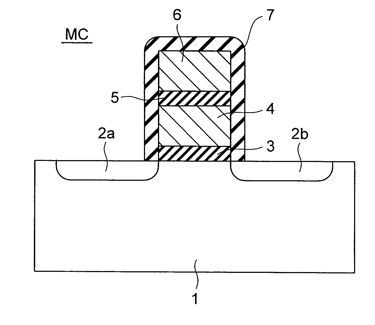
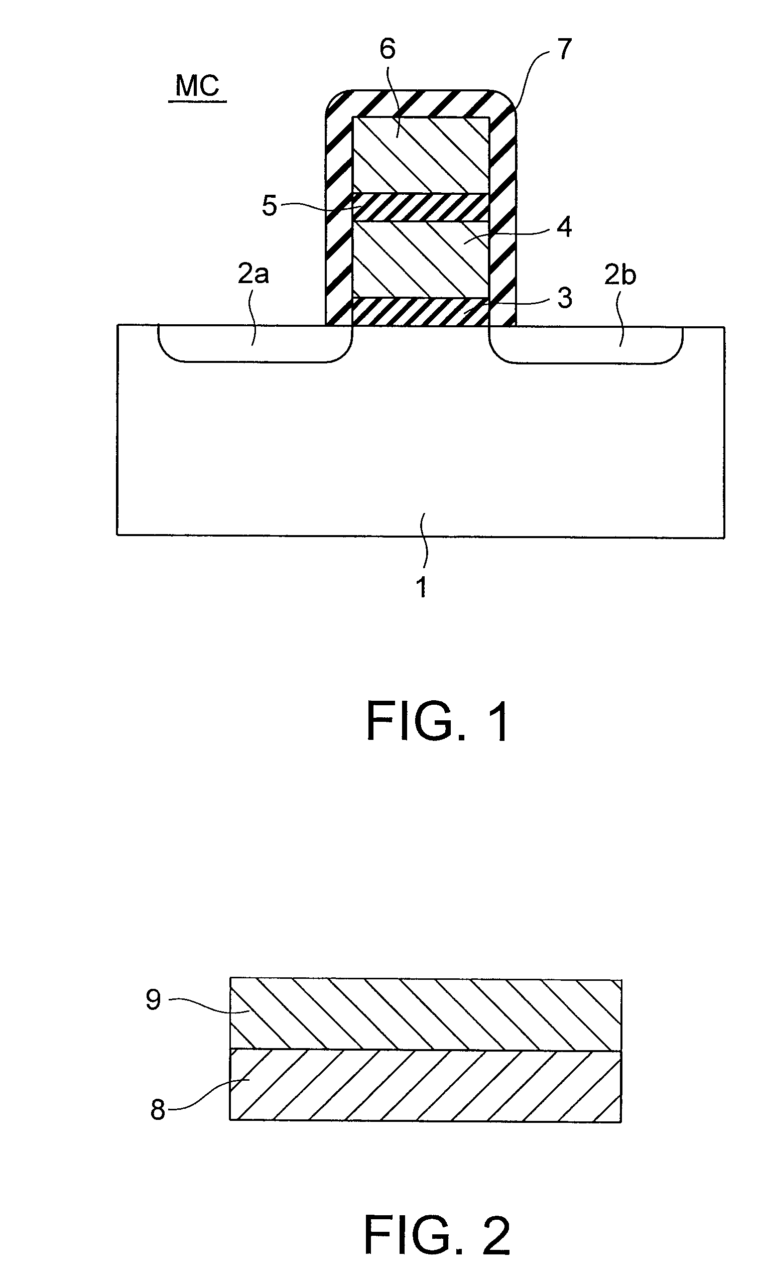
[0076]A nonvolatile semiconductor memory apparatus in accordance with a first embodiment of the present invention has NAND cell units arranged in a matrix form, for example. Each of the NAND cell units includes a NAND cell that is formed with memory cells connected in series. As shown in FIG. 1, each memory cell MC has n-type source and drain regions 2a and 2b that are formed at a distance from each other in a p-type Si substrate 1 and contain n-type impurities (such as P and As). A tunnel insulating film 3 is formed on the portion of the Si substrate 1 located between the source region 2a and the drain region 2b. A charge storage film 4 is formed on the tunnel insulating film 3, and an interelectrode insulating film 5 is formed on the charge storage film 4. A control gate electrode 6 is formed on the interelectrode insulating film 5. The gate of the stacked structure formed with the control gate electrode 6, the interelectrode insulating film 5, the charge storage film 4, and the t...

second embodiment

[0108]Next, a nonvolatile semiconductor memory apparatus in accordance with a second embodiment of the present invention is described. In the nonvolatile semiconductor memory apparatus of the first embodiment, the tunnel insulating film has the assist level formed only in the high-k layer. In the nonvolatile semiconductor memory apparatus of this embodiment, on the other hand, the tunnel insulating film has the assist level not only in the high-k layer but also in the low-k layer. The nonvolatile semiconductor memory apparatus of the second embodiment has the same structure as the nonvolatile semiconductor memory apparatus of the first embodiment, except for the tunnel insulating film.

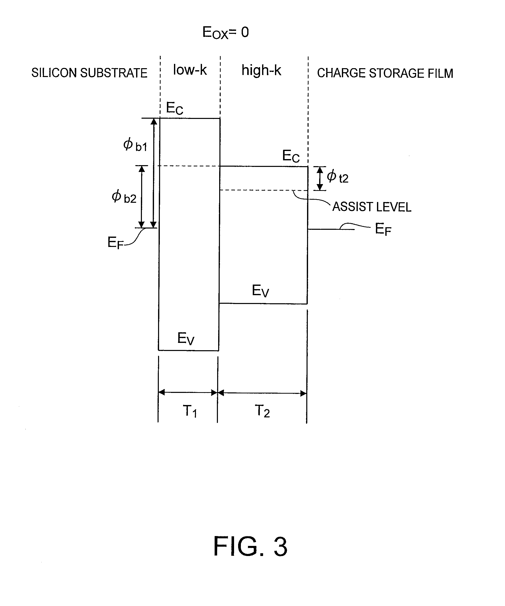
[0109]FIG. 12 is an energy band diagram of the tunnel insulating film of this embodiment observed when the electric field Eox is 0, with the assist level φt1 being added to the low-k layer shown in FIG. 3. FIGS. 13A and 13B schematically show the energy band observed in a case where a low electric fiel...

third embodiment

[0163]Referring now to FIGS. 51A to 52D, a method for manufacturing a FG-type nonvolatile memory in accordance with a third embodiment of the present invention is described. FIGS. 51A, 51C, 51E, 52A, and 52C are cross-sectional views that are orthogonal to the cross-sectional views of FIGS. 51B, 51D, 51F, 52B, and 52D, respectively.

[0164]First, as shown in FIGS. 51A and 51B, a tunnel insulating film 22 having the assist level described in the foregoing embodiments is formed on the surface of a p-type silicon substrate 1 that is doped with desired impurities. For example, after a SiO2 layer is formed by oxidizing the surface through combustion oxidation with the use of hydrogen and oxygen at 750° C., a HfO2 layer having Ge added thereto is formed by CVD (chemical vapor deposition), so as to obtain a tunnel insulating film having the assist level. A 60 nm thick phosphorus-doped crystalline silicon layer 23 to be the floating gate electrode is deposited by CVD. A mask member 24 formed ...


PUM


Abstract

A nonvolatile semiconductor memory apparatus includes: a memory element including: a semiconductor substrate; a source region and a drain region formed at a distance from each other in the semiconductor substrate; a first insulating film formed on a portion of the semiconductor substrate located between the source region and the drain region, having sites that perform electron trapping and releasing and are formed by adding an element different from a base material, and including insulating layers having different dielectric constants, the sites having a higher level than a Fermi level of a material forming the semiconductor substrate; a charge storage film formed on the first insulating film; a second insulating film formed on the charge storage film; and a control gate electrode formed on the second insulating film.

Description

CROSS-REFERENCE TO RELATED APPLICATION[0001]This application is based upon and claims the benefit of priority from prior Japanese Patent Application No. 2008-72148 filed on Mar. 19, 2008 in Japan, the entire contents of which are incorporated herein by reference.BACKGROUND OF THE INVENTION[0002]1. Field of the Invention[0003]The present invention relates to a nonvolatile semiconductor memory apparatus.[0004]2. Related Art[0005]In recent years, electrically writable and erasable nonvolatile semiconductor memory apparatuses have been developed to provide higher performances. As the nonvolatile semiconductor memory apparatuses, there are EEPROMs (Electrically Erasable Programmable Read Only Memories). Two typical examples of EEPROMs are of a floating gate type (hereinafter also referred to as the FG type) and a MONOS (Metal Oxide Nitride Oxide Semiconductor) type.[0006]The fundamental structure of a FG-type EEPROM is a stacked structure that includes, from the top layer, a control gate...

Claims


Application Information

Patent Timeline
IPC IPC(8): H01L29/792
CPCH01L27/11568H01L27/11521H10B43/30H10B41/30H01L29/517
Inventor KOIKE, MASAHIROMITANI, YUUICHIRONAKASAKI, YASUSHIKOYAMA, MASATO
Owner KIOXIA CORP
Why Eureka
Try Eureka