Method of manufacturing a device with a cavity

a manufacturing method and micro-device technology, applied in micro-structural devices, electrostatic generators/motors, generators/motors, etc., can solve the problems of air gaps between metal lines and large dielectric areas, methods that are less compatible with back-end-of-line (beol) processing, and achieve the effect of more beol-processing compatibility

Active Publication Date: 2009-10-29
TAIWAN SEMICON MFG CO LTD
View PDF4 Cites 118 Cited by
  • Summary
  • Abstract
  • Description
  • Claims
  • Application Information

AI Technical Summary

Benefits of technology

[0007]It is an object of the invention to provide a method of manufacturing a micro-device with a cavity that requires lower temperatures, and that is therefore more BEOL-processing compatible.
[0013]The effect of the features of the method in accordance with the invention is that no high temperature steps are needed anymore. The inventors have realized that some materials are permeable, or may be made permeable, to vapor HF etchant and the etch products and are substantially left intact by that etchant. Vapor HF etching may be done at relatively low temperatures, i.e. 35° C., leaving a higher temperature budget for other processing steps which may be done in between. Also the deposition of the porous layer is done at relatively low temperatures. This renders the method more compatible with BEOL processing wherein temperatures are preferably kept well below 450° C. In the method it is important that a material is selected that is not etched, or substantially left in tact, by vapor-HF and that is porous enough to remove the “sacrificial” oxide underneath the porous layer by the vapor HF etchant and also permeable for the etch products. The inventors have realized that this combination of features can be used for creating a cavity underneath the porous layer.
[0020]in the step of selectively etching, both the sacrificial oxide region and the further sacrificial oxide region are selectively etched for forming the cavity around the element for releasing the element so as to obtain the component. The method in accordance with the invention is advantageously applied in the manufacture of MEMS devices, and in particular in the encapsulation stage thereof. In this embodiment the lower temperature of the process in accordance with the invention, leads to a higher compatibility with BEOL processing. Also, the method renders the need for etching holes in the porous layer superfluous (which is done in other known methods). This saves a masking step and thus costs. An additional advantage in the manufacture of MEMS device is that the porous layer makes it much easier to seal the cavity. The porous layer prevents deposition of sealing material in the cavity (and on the moveable component).
[0024]in the step of selectively etching, the etching occurs through the porous layer which is located in the release hole. This embodiment of the method looks more like the conventional method, because it makes use of the packaging cap layer, which is used in the conventional methods too. The use of the packaging cap layer provides for a better mechanical strength / stability of the structure (i.e. the packaging cap layer is much stronger than the porous layer). The porous layer may be provided on a wall or on the walls of the release hole or maybe covering the release hole as a lid.
[0033]in the step of selectively etching, the first cavity in the first interconnect layer and a second cavity in the second interconnect layer are obtained for forming airgaps. This method results in a semiconductor device having multiple interconnect layers, which provides for more routing resources and higher packing densities. The advantages of the method in accordance with the invention are significant. First of all, all airgaps are formed in the last BEOL step, which ensures a higher structural integrity during back-end processing. Furthermore, the airgaps are formed in a single etch step which reduces the number of processing steps.

Problems solved by technology

Because of mechanical reasons such technologies are not yet feasible, but as an intermediate solution technologies have been reported wherein cavities, also being referred to as air-gaps, are present in the interconnect layers.
Then, the disposable layer decomposes and disappears through the permeable dielectric layer, leaving air gaps behind in between the metal lines and the large dielectric areas.
A problem with the known method of manufacturing a micro device with a cavity is that the method requires, in particular in the step of decomposing the sacrificial layer, relatively high temperatures (150-450° C.) which makes the method less compatible with back-end-of-line (BEOL) processing.
This decomposing temperature limits the processing after deposition.

Method used


Image

  • Method of manufacturing a device with a cavity
  • Method of manufacturing a device with a cavity
  • Method of manufacturing a device with a cavity

Examples


first embodiment

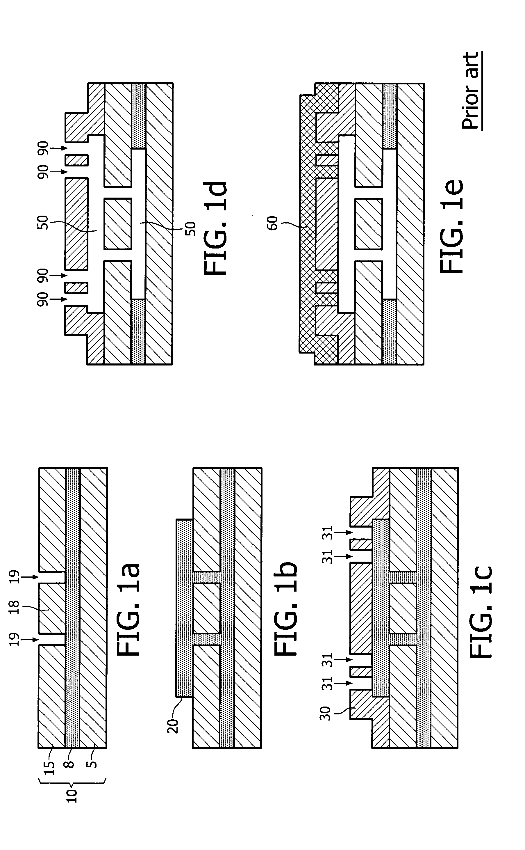
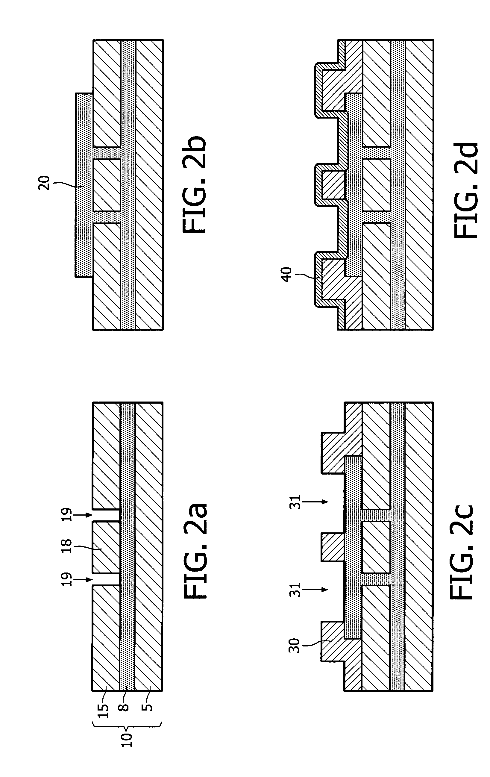
[0072]FIGS. 2a to 2f schematically show an encapsulation process of a MEMS device in accordance with the method of the invention. This process will be discussed in as far as it differs from the known process illustrated in FIGS. 1a to 1e. The first two steps (FIGS. 2a and 2b) are the same as the first two steps of the known process. The third step, illustrated in FIG. 2c differs from the third step of the known method in that the release holes 31′ in the packaging cap layer 30 may be designed much larger and may also be located above the moveable component 18. In the step of FIG. 2a, if the sacrificial oxide layer 8 is not an oxide it has to be removed before the sacrificial oxide layer 20 is deposited, because it will have to be removed together with the sacrificial oxide layer 20.

[0073]The step of FIG. 2d is new. In this step a porous layer 40 is deposited on the packaging cap layer 30 and in the release holes. The inventors have discovered that the material of the porous layer 40...

second embodiment

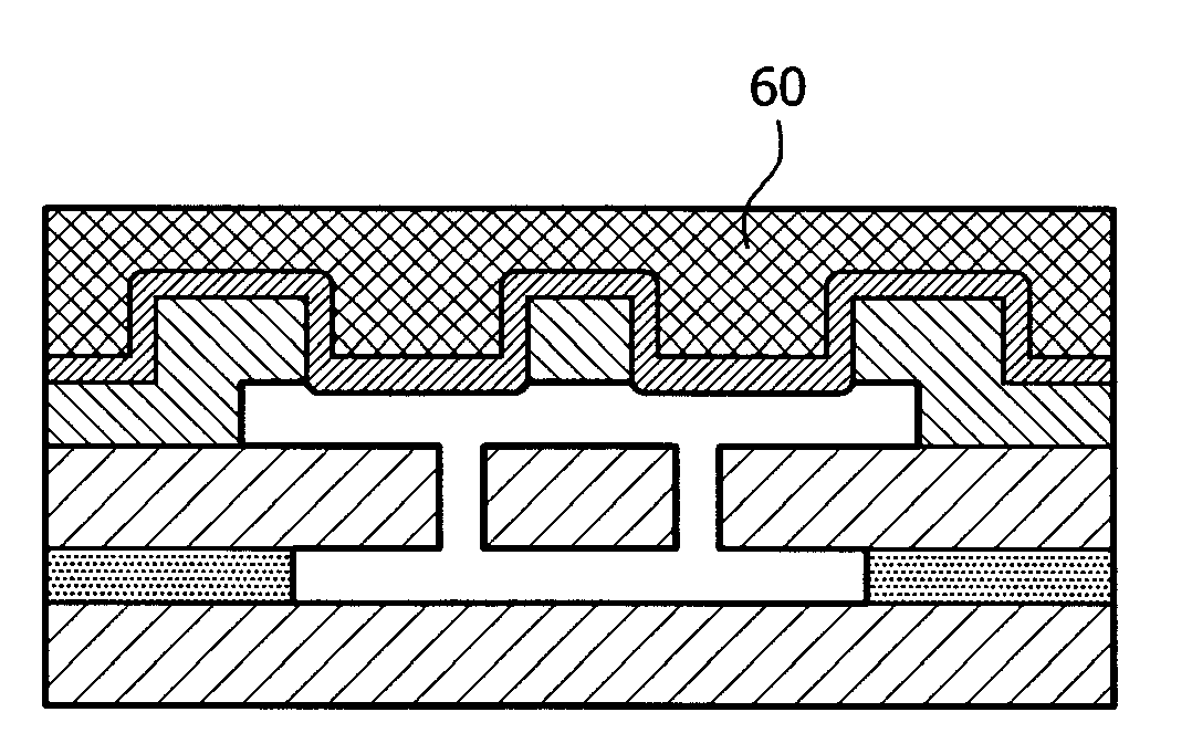
[0084]FIGS. 6a1 and 6a2 schematically show an etching step carried out between two process stages of a first experiment proving the feasibility of the method of the invention. FIGS. 6b to 6d show cross-section SEM pictures of devices in accordance with FIG. 6a2 for different porous layer thicknesses, 700 nm, 500 nm, and 300 nm, respectively. In FIG. 6a1 the porous layer 30 is directly used as packaging cap layer. The most important result of this second experiment is that even a 700 nm thick BD layer was porous enough to remove the sacrificial (oxide) layer 20 as is visible in FIG. 6b. The BD layer must be chosen thick enough to withstand the deposition of a sealing layer 60 (FIG. 5), which also depends on the sealing requirements.

third embodiment

[0085]FIGS. 7a to 7j show different stages in a method of manufacturing a semiconductor device in accordance with the method of the invention.

[0086]In the step of FIG. 7a a substrate 110 is provided comprising a semiconductor body 105. The semiconductor body 105 may comprise any one of the following semiconductor materials and compositions like silicon (Si), germanium (Ge), silicon germanium (SiGe), gallium-arsenide (GaAs) and other III-V compounds like indium-phosphide (InP), cadmium sulfide (CdS) and other II-VI compounds, or combinations of these materials and compositions. The semiconductor body may comprise active elements like transistors and diodes (not shown). These active elements together may form an electronic circuit (not shown). In any case, connection of the active elements is done via interconnect layers. These interconnect layers have parasitic capacitances which are defined by the dielectric constant of surrounding materials. The semiconductor body may even comprise...


PUM

PropertyMeasurementUnit
dielectric constantaaaaaaaaaa
temperatureaaaaaaaaaa
temperaturesaaaaaaaaaa

Abstract

The invention relates to a micro-device with a cavity (50), the micro-device comprising a substrate (10, 110), the method comprising steps of: A) providing the substrate (10, 110), having a surface and comprising a sacrificial oxide region (20, 107, 115) at the surface ( ); B) covering the sacrificial oxide region (20, 107, 115) with a porous layer (40, 114, 124) being permeable to a vapor HF etchant (100), and C) selectively etching the sacrificial oxide region (20, 107, 115) through the porous layer (40, 114, 124) using the vapor HF etchant (100) to obtain the cavity (50). This method may be used in the manufacture of various micro-devices with a cavity (50), i.e. MEMS devices, and in particular in the encapsulation part thereof, and semiconductor devices, and in particular the BEOL-part thereof.

Description

CROSS REFERENCE[0001]This application claims priority to European patent application number 08103686.5, filed Apr. 23, 2008, the disclosure of which is incorporated herein by reference.FIELD OF THE INVENTION[0002]The invention relates to a method of manufacturing a micro-device with a cavity. The invention further relates to such micro-device with a cavity, and in particular to a MEMS device or a semiconductor device.BACKGROUND OF THE INVENTION[0003]Various types of micro-devices with a cavity exist. A first class of such micro-devices consists of micro-electromechanical system (MEMS) devices. Such devices generally comprise a moveable element that is controlled by electro-static or piezo-electric forces, i.e. a resonator or moveable electrode. In order to allow the element to be moveable such element is preferably arranged within a cavity.[0004]A second class of such micro-devices consists of semiconductor devices having at least one interconnect layer. In order to reduce parasitic...

Claims


Application Information

Patent Timeline
Patent Type & Authority Applications(United States)
IPC IPC(8): H01L29/84H01L21/50
CPCB81C1/00476H01L21/02H01L21/02126H01L29/84H01L21/31116H01L21/50H01L21/76813H01L21/7682H01L21/76849H01L2221/1036H01L21/7688H02N1/00
Inventor VERHEIJDEN, GREJA JOHANNA ADRIANA MARIADAAMEN, ROELKOOPS, GERHARD
Owner TAIWAN SEMICON MFG CO LTD
Why Eureka
Try Eureka