Semiconductor device and method for manufacturing the same

a technology of semiconductor devices and semiconductors, applied in semiconductor devices, semiconductor/solid-state device details, electrical apparatus, etc., can solve the problems of thickness and larger size of semiconductor devices, and achieve the effects of high yield, reduced thickness, and high reliability

Active Publication Date: 2009-10-29
SEMICON ENERGY LAB CO LTD
View PDF39 Cites 268 Cited by
  • Summary
  • Abstract
  • Description
  • Claims
  • Application Information

AI Technical Summary

Benefits of technology

[0025]With a pair of impact resistance layers which sandwich a semiconductor integrated circuit, and an impact diffusion layer provided to be stacked on the semiconductor integrated circuit, a highly reliable semiconductor device wh

Problems solved by technology

However, there is a problem in that a semiconductor device becomes to be thi

Method used


Image

  • Semiconductor device and method for manufacturing the same
  • Semiconductor device and method for manufacturing the same
  • Semiconductor device and method for manufacturing the same

Examples


embodiment 1

[0049]In this embodiment, a highly reliable semiconductor device and a method for manufacturing a semiconductor device with a high yield will be described in detail with reference to FIGS. 1A to 1C, FIGS. 2A and 2B, and FIGS. 3A to 3D.

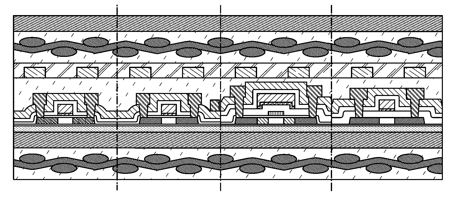
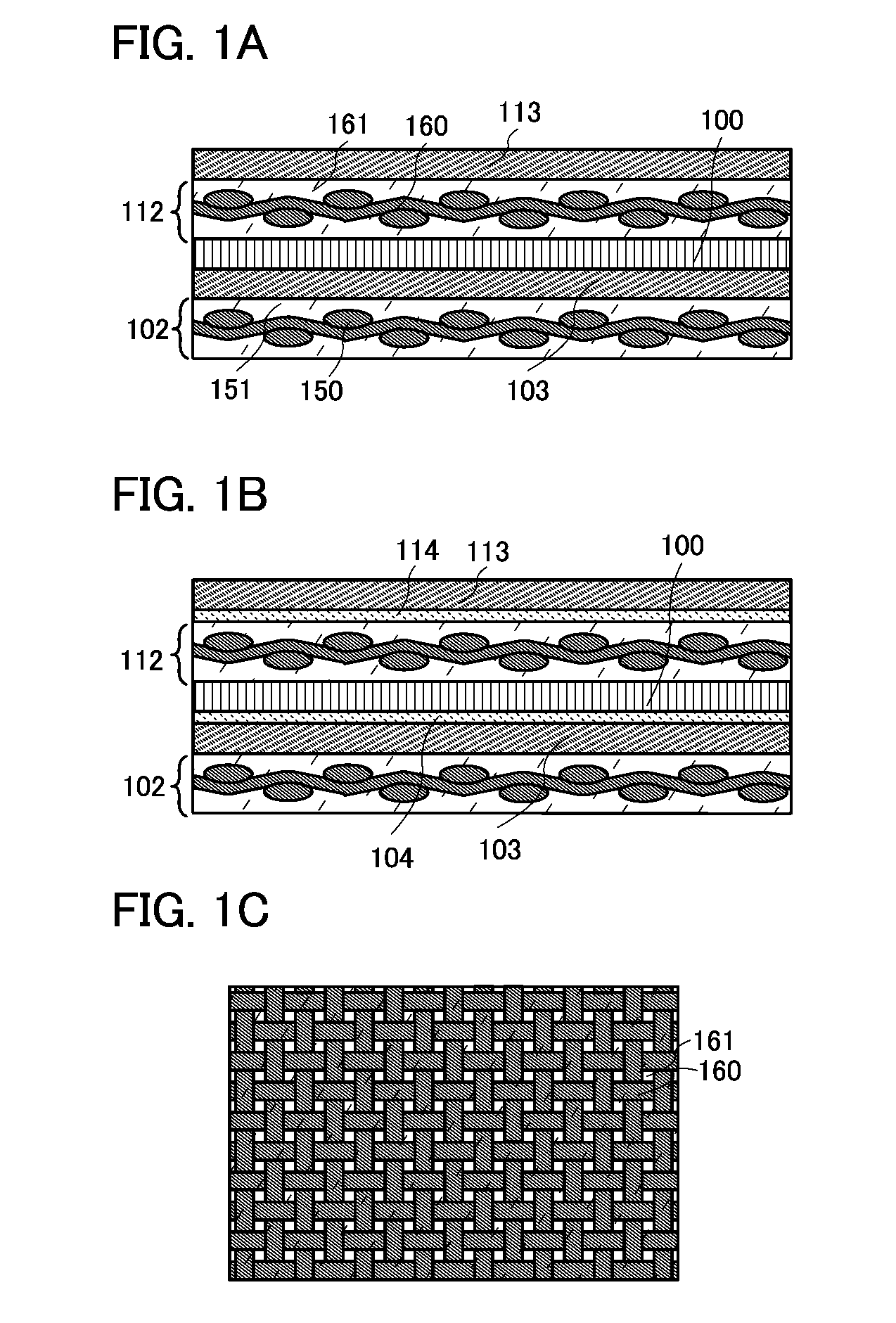
[0050]In a semiconductor device of this embodiment, a semiconductor integrated circuit is separated from a substrate which is used for formation of the semiconductor integrated circuit and sandwiched between impact resistance layers having flexibility. Note that, the substrate over which the semiconductor integrated circuit is formed is also referred to as a formation substrate. Accordingly, the semiconductor integrated circuit is formed over the formation substrate with a separation layer interposed therebetween.

[0051]FIGS. 1A and 1B each illustrate a semiconductor device of this embodiment. In FIG. 1A, a semiconductor integrated circuit 100 is sandwiched between a first impact resistance layer 112 and a first impact diffusion layer 113, and a second ...

embodiment 2

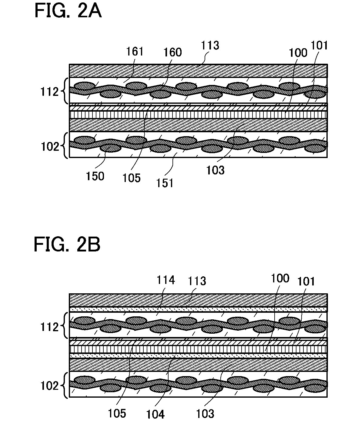
[0093]In this embodiment, a highly reliable semiconductor device and a method for manufacturing a semiconductor device with a high yield will be described in detail with reference to FIGS. 4A to 4C and FIGS. 5A to 5C. Here, as an example of a semiconductor device, a complementary metal oxide semiconductor (CMOS) will be described.

[0094]A transistor 210 and a transistor 211 are formed over a substrate 200 having an insulating surface, which is a formation substrate, with a separation layer 201 and a base insulating layer interposed therebetween, and an insulating film 212, an insulating film 213, and an insulating film 214 are provided thereover, whereby a semiconductor integrated circuit 250 is formed (see FIG. 4A).

[0095]The transistor 210 is a thin film transistor which includes source and drain regions 224a and 224b, impurity regions 223a and 223b which contains an impurity at lower concentration than the source and drain regions 224a and 224b, a channel formation region 226, a ga...

embodiment 3

[0128]In this embodiment, an example of a semiconductor device having a memory, as a semiconductor device which achieves higher integration and further reduction in thickness and size, and a manufacturing method thereof will be described with reference to FIGS. 6A to 6E, FIGS. 7A to 7C, and FIGS. 8A and 8B.

[0129]A semiconductor device of this embodiment includes a memory including a memory cell array and a driver circuit portion which drives the memory cell array.

[0130]A separation layer 301 is formed over a substrate 300 which is a formation substrate having an insulating surface, and an insulating film 302 serving as a base film is formed over the separation layer 301.

[0131]Next, a semiconductor film is formed over the insulating film 302. The semiconductor film may be formed by a sputtering method, an LPCVD method, a plasma CVD method or the like to be 25 to 200 nm thick (preferably, 30 to 150 nm thick).

[0132]In this embodiment, an amorphous semiconductor film is formed over the ...


PUM


Abstract

In a semiconductor integrated circuit sandwiched between a pair of a first impact resistance layer and a second impact resistance layer, an impact diffusion layer is provided between the semiconductor integrated circuit and the second impact resistance layer. By provision of the impact resistance layer against the external stress and the impact diffusion layer for diffusing the impact, force applied to the semiconductor integrated circuit per unit area is reduced, so that the semiconductor integrated circuit is protected. The impact diffusion layer preferably has a low modulus of elasticity and high breaking modulus.

Description

TECHNICAL FIELD[0001]The present invention relates to semiconductor devices and methods for manufacturing the same.BACKGROUND ART[0002]It is important to increase strength against stress from the outside, for semiconductor integrated circuit chips (also referred to as IC chips) with which reduction in thickness and size is attempted.[0003]In order to increase the strength of the chips, a variety of methods for reinforcing the chips are proposed (see Reference 1: Japanese Published Patent Application No. 2006-139802). For example, in Reference 1, a method in which a chip is sandwiched between reinforcement metal plates and covered with a sealing resin to be hardened is reported.DISCLOSURE OF INVENTION[0004]However, there is a problem in that a semiconductor device becomes to be thick and to have a larger size by provision of the reinforcement metal plates.[0005]Accordingly, an object of an embodiment of the present invention is to provide a highly reliable semiconductor device which ...

Claims


Application Information

Patent Timeline
IPC IPC(8): H01L23/29H01L21/56
CPCH01L21/561H01L21/568H01L2924/0002H01L21/6835H01L23/295H01L23/3114H01L2221/6835H01L2924/12044H01L2924/14H01L2924/19041H01L2924/19043H01L2924/30105H01L23/293H01L23/562H01L2924/00H01L27/12H01L27/1203H01L21/02164H01L21/0214
Inventor EGUCHI, SHINGO
Owner SEMICON ENERGY LAB CO LTD
Why Eureka
Try Eureka