

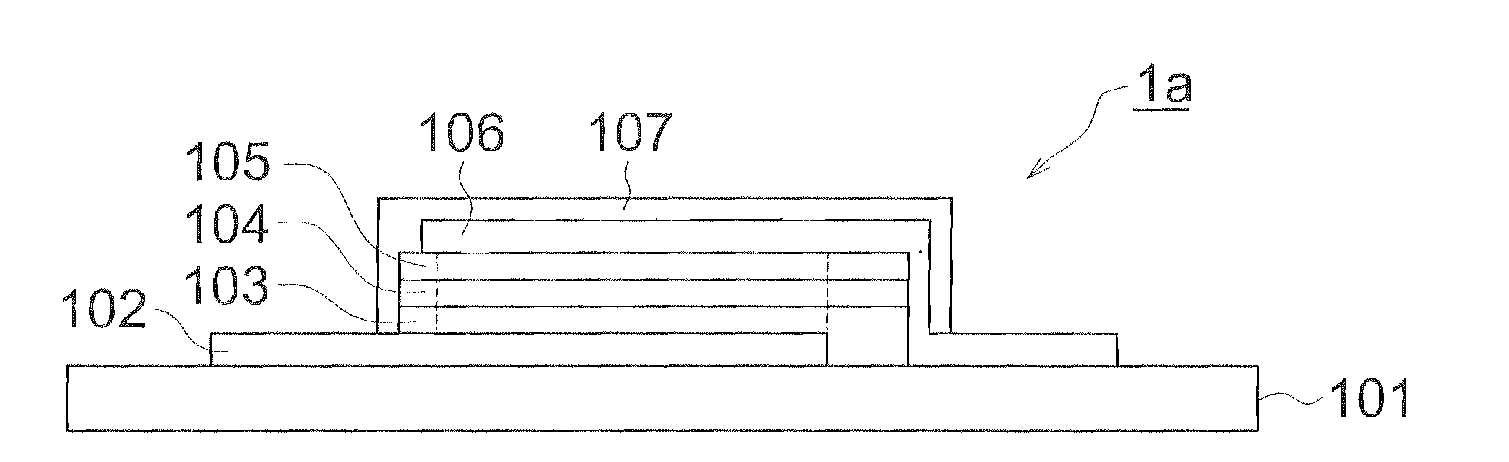
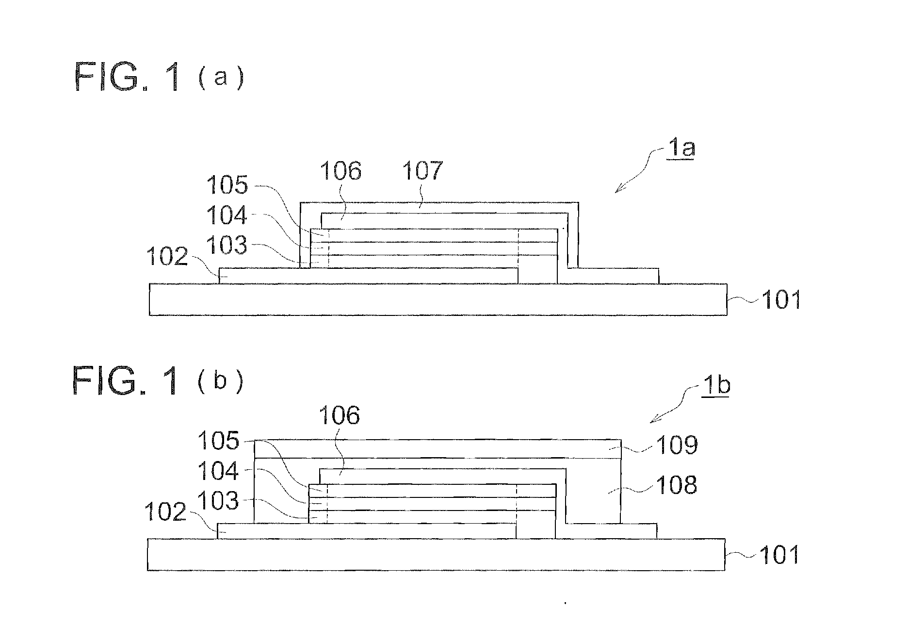
Process for Producing Organic Electroluminescent Element and Organic Electroluminescent Display Device
a technology of electroluminescent elements and production methods, applied in the direction of discharge tube luminescnet screens, sustainable manufacturing/processing, final product manufacturing, etc., can solve the problems of high cost, difficult vacuum evaporation manufacturing, and complicated operation of low molecular weight type materials. achieve the effect of stable performance quality and high production efficiency
- Summary
- Abstract
- Description
- Claims
- Application Information
AI Technical Summary
Benefits of technology
Problems solved by technology
Method used
Image

Examples
example 1
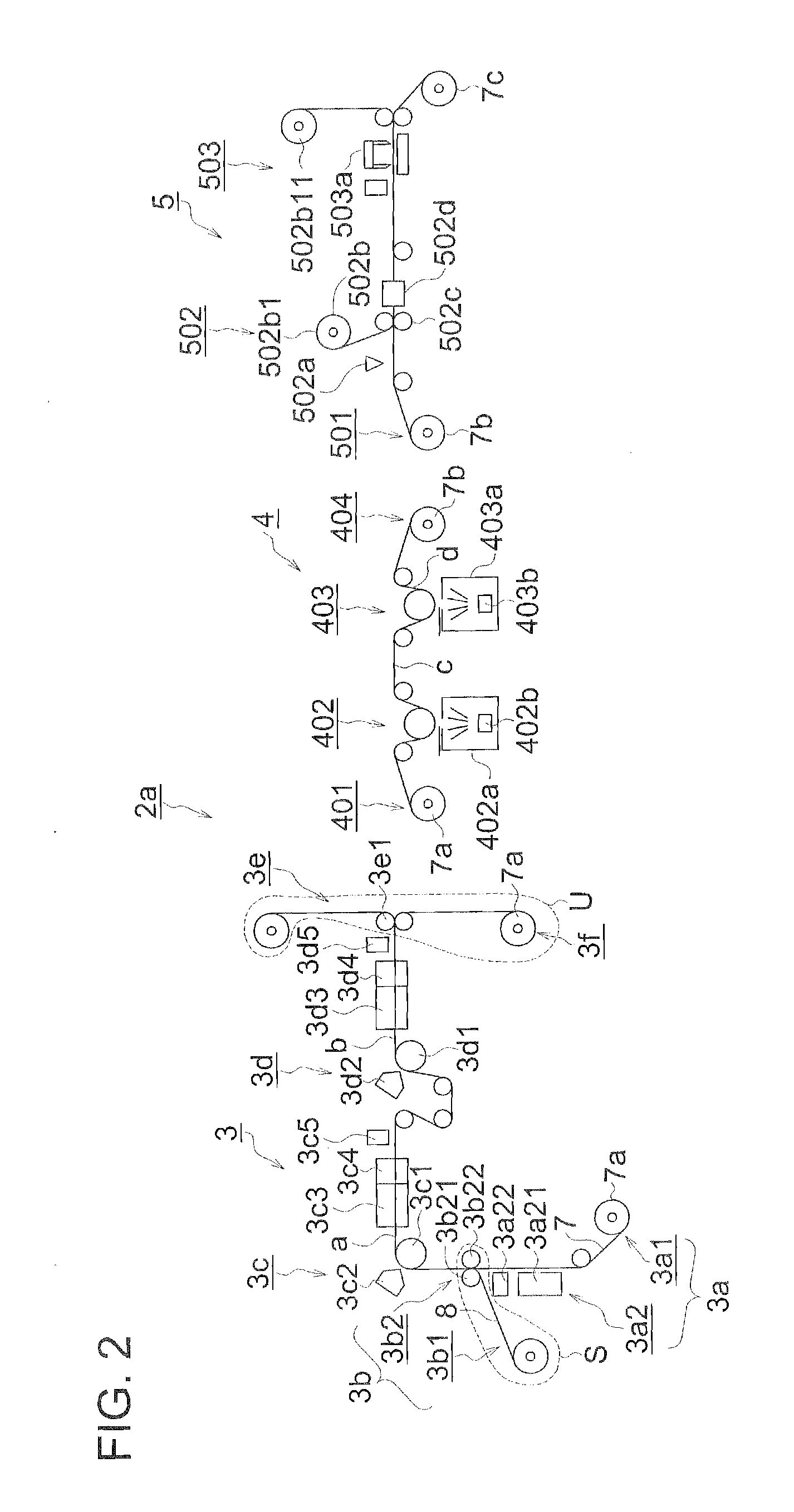
Preparation of Band-Form Flexible Support
[0183]Polyether sulfon (film manufactured by Sumitomo Bakelite Co., Ltd., hereinafter, being abbreviated as PES) having a thickness of 200 μm and a width of 250 mm was prepared.
[0184](Preparation of Transparent Gas Barrier Layer)
[0185]Transparent gas barrier film in which three units comprising a low density layer, a medium density layer, a high density layer and a medium density layer were accumulated on the prepared PES by means of a plasma discharge treatment method, was prepared. A moisture permeability measured by means of a method based on JIS K 7129-1992 was not higher than 10−3 g / (m2·24 h). An oxygen permeability measured by means of a method described in JIS K 7126-1987 was not higher than 10−3 ml / (m2·24 hr-MPa).
[0186](Preparation of Band-Form Flexible Support Bearing First Electrode)
[0187]On the formed barrier layer, after ITO (indium tin oxide) having a thickness of 120 nm was formed by an evaporation method so as to form a first e...
example 2
Preparation of Band-Form Flexible Support Bearing First Electrode
[0225]By utilizing a band-form flexible support similar to example 1, a transparent gas barrier layer and a first electrode were formed under the same condition, whereby a band-form flexible support bearing a first electrode identical with that of example 1 was prepared.
[0226](Preparation of Masking Member)
[0227]Polyester film having a thickness of 25 μm as a substrate and silicone type resin as an adhesive were utilized, and masking members of 100 m each varying adhesive strength were prepared to be Nos. 2-a-2-f. Herein, adhesive strength indicates a value measured based on a measurement of adhesion force defined by JIS Z-0237 adhesive tape-adhesive sheet test method. Variation of adhesion force was made by varying the composition of an adhesive layer. Herein, the width of a masking member was 25 mm.
TABLE 3Masking memberAdhesive strengthNo.(N / 25 mm)2-a0.82-b1.02-c4.22-d6.92-e10.02-f11.8
[0228](Lamination of Masking Mem...
PUM
| Property | Measurement | Unit |
|---|---|---|
| Energy | aaaaa | aaaaa |
| Length | aaaaa | aaaaa |
| Length | aaaaa | aaaaa |
Abstract
Description
Claims
Application Information