Silicon structure having an opening which has a high aspect ratio, method for manufacturing the same, system for manufacturing the same, and program for manufacturing the same, and method for manufacturing etching mask for the silicon structure

a technology of silicon structure and aspect ratio, which is applied in the field of silicon structure having an opening, can solve the problems of unflagging demand for formation of an opening with a high aspect ratio, unavoidable etching of silicon oxide film, and wide opening width, etc., and achieve high aspect ratio, prevent corrosion of an etched portion, and high aspect ratio

Inactive Publication Date: 2009-11-05
SUMITOMO PRECISION PROD CO LTD
View PDF8 Cites 52 Cited by
  • Summary
  • Abstract
  • Description
  • Claims
  • Application Information

AI Technical Summary

Benefits of technology

[0053]A silicon structure according to the present invention can have an opening which has a high aspect ratio, and by employing a manufacturing method, a manufacturing system, and a manufacturing program according to the present invention, the silicon structure having an opening which has a high aspect ratio can be manufactured by using a silicon material. In addition, by employing a method according to the present invention for manufacturing an etching mask, the etching mask which allows prevention of corrosion of an etched portion of a sidewall upon etching the silicon and also prevention of depletion of the etching mask under the etching can be manufactured. As a result, the invention of the method for manufacturing this etching mask enables manufacture or reproduction of the etching mask for forming an opening which has a high aspect ratio, in the silicon material.

Problems solved by technology

Despite the dramatic progress, however, a demand for formation of an opening which has a high aspect ratio remains unflagging.
In this method, however, a sidewall protection film in the vicinity of a topmost surface of a silicon substrate (hereinafter, also referred to as a substrate topmost surface) which has not been etched is destroyed due to oblique incidence of ions or the like, thereby incurring a problem that a width of the opening is made wider than its initial width or a surface of the sidewall is roughened.
In such as case, as described in the above-mentioned Patent Document, even when the silicon oxide film is used as an etching mask, it is unavoidable for this silicon oxide film to be etched.
This phenomenon occurs, regardless of whether the mask is a resist or the silicon oxide film, and needless to say, the consumption is drastic when the resist is used.
Thus, in a case where a particularly high aspect ratio is demanded, the above technology cannot be applied.
As described above, when a silicon structure having an opening which has a high aspect ratio is manufactured, merely solving the problem of the corrosion on the sidewall is not enough but it is required to take into account depletion of the mask.
In a case where an aspect ratio is greater than or equal to 40 when trench etching is performed, or an aspect ratio is greater than or equal to 20 when hole etching is performed, the above-described problems particularly emerge.

Method used


Image

  • Silicon structure having an opening which has a high aspect ratio, method for manufacturing the same, system for manufacturing the same, and program for manufacturing the same, and method for manufacturing etching mask for the silicon structure
  • Silicon structure having an opening which has a high aspect ratio, method for manufacturing the same, system for manufacturing the same, and program for manufacturing the same, and method for manufacturing etching mask for the silicon structure
  • Silicon structure having an opening which has a high aspect ratio, method for manufacturing the same, system for manufacturing the same, and program for manufacturing the same, and method for manufacturing etching mask for the silicon structure

Examples


first embodiment

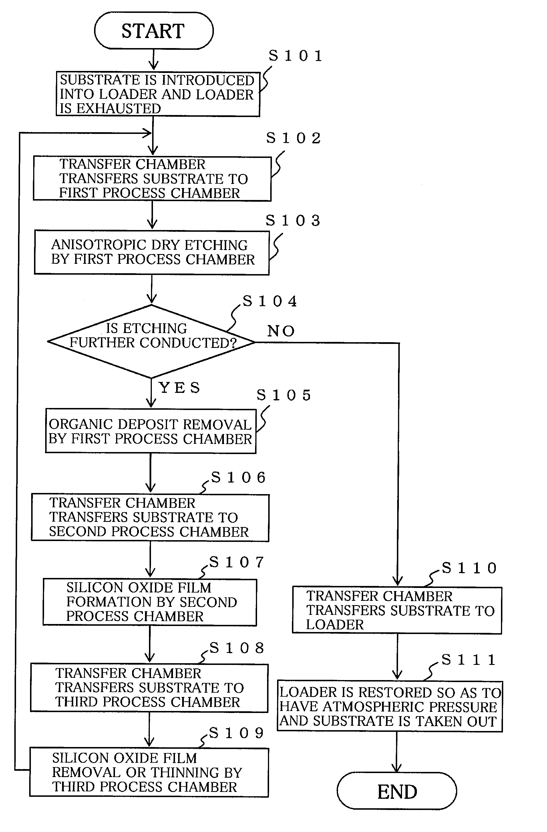
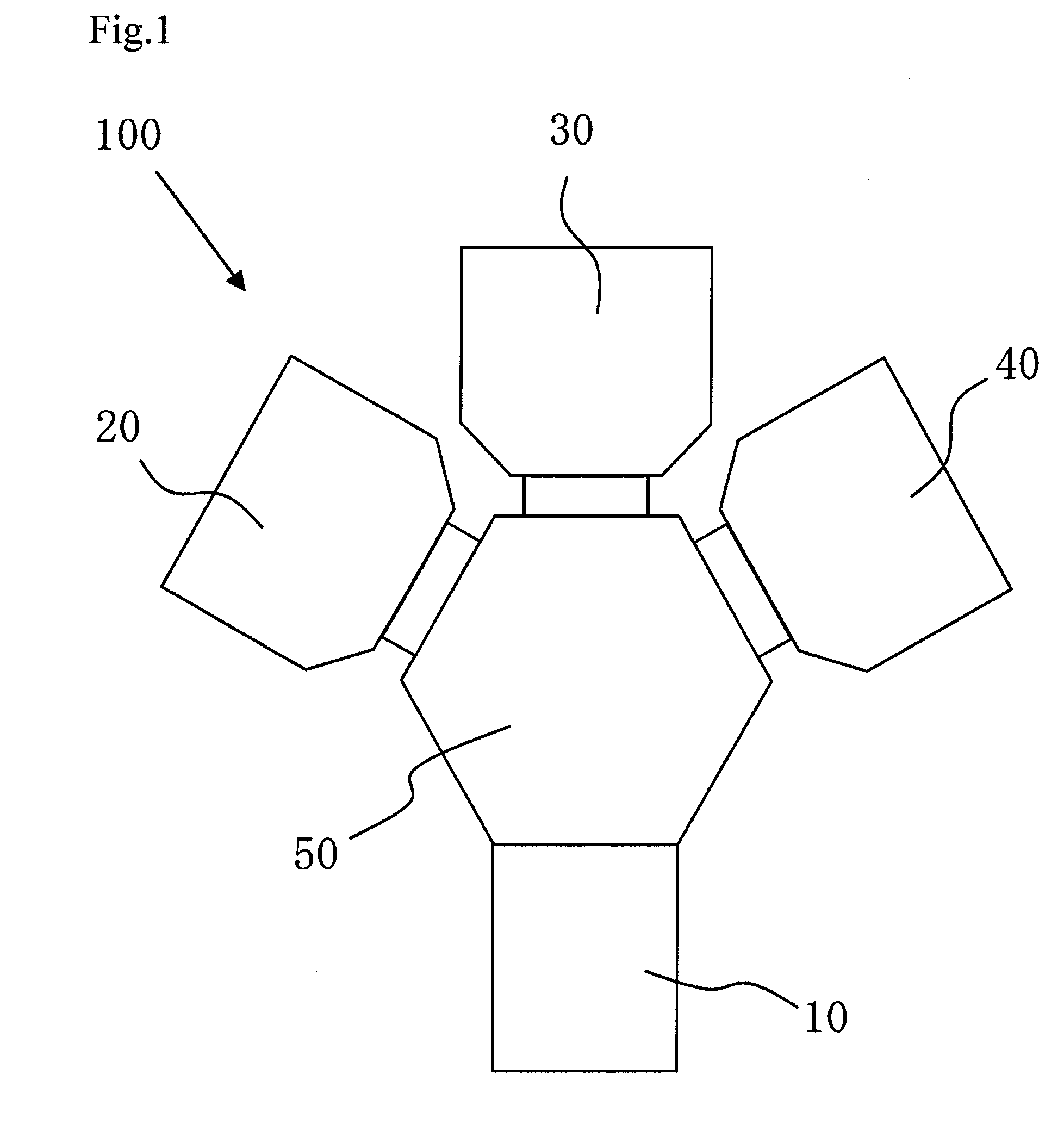
[0077]FIG. 1 shows a top view of a silicon structure manufacturing system of the present embodiment. Since FIG. 1 is a schematic diagram, peripheral units such as gas supply mechanisms and exhaust mechanisms of respective chambers are not shown. The silicon structure manufacturing system 100 comprises: three process chambers 20, 30, and 40 having closed spaces; one loader 10; and one transfer chamber 50. Here, the first process chamber 20 is used for performing anisotropic etching of silicon and for performing etching to remove an organic deposit. The organic deposit includes a resist mask and a sidewall deposited film which is formed by etching. In addition, the second process chamber 30 is used for forming a silicon oxide film on a surface of the mask and an inner wall of an etched portion by a CVD method. Lastly, the third process chamber 40 is used for removing or thinning a part of the above-mentioned oxide film by using a gas containing a vapor of hydrogen fluoride.

[0078]An ou...

second embodiment

[0101]A silicon structure manufacturing system according to the present embodiment has the same system configuration as that shown in FIG. 1 except that the first process chamber 20 shown in FIG. 1 is replaced with an RIE apparatus 70 shown in FIG. 7. Only in the description of the present embodiment, the RIE apparatus 70 is referred to as a first process chamber for convenience sake. Also in the description of the present embodiment, common reference numerals are used to denote common parts throughout all the associated drawings. In the drawings, the illustrated elements of the present embodiment are not necessarily to scale. Flow rates of the below-mentioned gases are those in standard conditions.

[0102]Next, processes in the present embodiment will be described mainly with reference to FIG. 7, FIG. 8A through FIG. 8F, and FIG. 9. Accordingly, the descriptions regarding the system configuration shown in FIG. 3 and FIG. 4, to which the description of the present embodiment is also g...


PUM

PropertyMeasurementUnit
aspect ratioaaaaaaaaaa
widthaaaaaaaaaa

Abstract

Provided are a silicon structure having an opening which has a high aspect ratio and an etching mask for forming the silicon structure. A step of performing hole etching or trench etching of silicon so as to substantially expose a portion of at least a bottom surface of etched silicon and a step of forming a silicon oxide film by a CVD method on the silicon structure formed by the step of performing the hole etching or the trench etching are conducted. Thereafter, a step of exposing the formed silicon oxide film to a gas containing a hydrogen fluoride vapor is conducted. Further, the above-mentioned step of performing the hole etching or the trench etching is conducted again.

Description

TECHNICAL FIELD[0001]The present invention relates to a silicon structure having an opening which has a high aspect ratio; a method for manufacturing the same; a system for manufacturing the same; and a program for manufacturing the same; and a method for manufacturing an etching mask for the silicon structure having an opening which has a high aspect ratio.BACKGROUND ART[0002]Technical fields in which MEMS (Micro Electro Mechanical Systems) devices utilizing silicon are applied have been rapidly evolving and in recent years, have been applied not only to micro turbines and sensors but also in information and communication fields and medical fields. One of principal element technologies which underlie this MEMS technology is anisotropic dry etching of silicon. It can be said that development of this element technology plays supporting roles in development of the MEMS technology. Over the last several years, the technology of the anisotropic dry etching of the silicon has made dramat...

Claims


Application Information

Patent Timeline
Patent Type & Authority Applications(United States)
IPC IPC(8): H01L21/3065C23C16/40C23F1/00H01L21/316G06F17/00
CPCC23C16/045H01L21/02057H01L21/02164H01L21/02271H01L21/31612H01L21/30655H01L21/3086H01L21/31116H01L21/3065
Inventor TANAKA, MASAHIKOOISHI, AKIMITSU
Owner SUMITOMO PRECISION PROD CO LTD
Why Eureka
Try Eureka