LED light source unit
- Summary
- Abstract
- Description
- Claims
- Application Information
AI Technical Summary
Benefits of technology
Problems solved by technology
Method used
Image

Examples
example 1
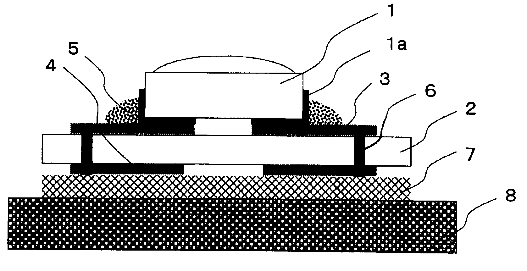
[0096]An LED light source unit of the type shown in FIG. 1 was prepared. Namely, with a glass cloth-incorporated printed board having a copper foil with a thickness of 35 μm formed on each side of an epoxy resin cloth impregnated with a glass base material with a thickness of 100 μm, through-holes were formed at predetermined positions (positions to connect a conductor circuit connected to an electrode terminal 1a of LED and a rear side conductor circuit located immediately therebelow) and copper-plated, and then, a conductor circuit on which LED is to be mounted, and a rear side conductor circuit to dissipate heat and to light up LED, was formed to obtain a printed board.
[0097]To 90 mass % of 2-ethylhexyl acrylate (“2EHA”, manufactured by TOAGOSEI CO., LTD.) having 10 mass % of acrylic rubber (“AR-53L”, manufactured by ZEON CORPORATION) dissolved therein, 10 mass % of acrylic acid (“AA”, manufactured by TOAGOSEI CO., LTD.) was mixed. To the mixture, 0.5 mass % of a photopolymerizat...
example 2
[0125]An LED light source unit was prepared in the same manner as in Example 1 except for the following. Namely, as an inorganic filler, aluminum oxide (“DAW-10”, manufactured by Denki Kagaku Kogyo Kabushiki Kaisha) was classified by a sieve of 45 μm to obtain an inorganic filler A having a maximum particle size of at most 45 μm and an average particle size of 9 μm. And, 40 vol % of the inorganic filler A, 45 vol % of the resin composition A and 15 vol % of the resin composition B were mixed to obtain a resin composition D.
[0126]Then, the resin composition D subjected to defoaming treatment was applied on a PET film having a thickness of 75 μm and having release treatment applied to its surface, and further, a PET film having release treatment applied to its surface was covered thereon, whereupon ultraviolet rays with a wavelength of 365 nm were applied to both sides at a dose of 3,000 mJ / cm2. Thereafter, heat treatment was carried out at 100° C. for 3 hours to cure the resin compos...
example 3
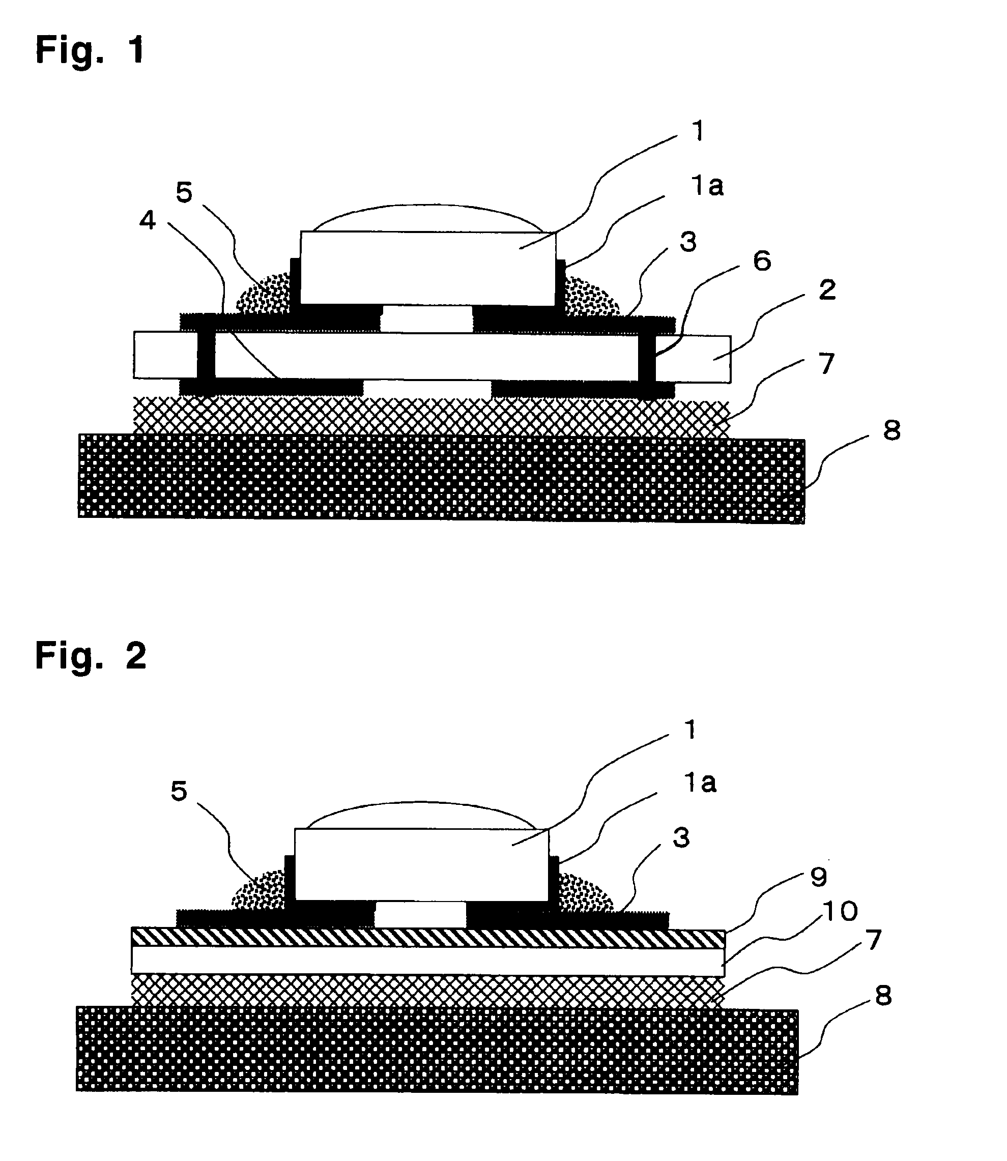
[0129]An LED light source unit was prepared in the same manner as in Example 1 except for the following.
[0130]Namely, using the same resin composition D as used in Example 2, the resin composition D subjected to defoaming treatment was applied in a thickness of 46 μm on a PET film having a thickness of 75 μm and having release treatment applied to its surface, and glass cloth having a thickness of 50 μm was laminated thereon, and further, a PET film having release treatment applied to its surface was covered and laminated thereon to impregnate the glass cloth with the resin composition D.
[0131]Then, ultraviolet rays of 365 nm were applied to both sides at a dose of 3,000 mJ / cm2. Then, heat treatment was carried out at 100° C. for 3 hours to cure the resin composition D thereby to obtain an electrically insulating thermally conductive adhesive tape having a thickness of 150 μm.
[0132]Then, cream solder (M705, manufactured by Senju Metal Industry Co., Ltd.) was applied by screen printi...
PUM
 Abstract
Description
Claims
Application Information
 - R&D
- Intellectual Property
- Life Sciences
- Materials
- Tech Scout
- Unparalleled Data Quality
- Higher Quality Content
- 60% Fewer Hallucinations
Browse by: Latest US Patents, China's latest patents, Technical Efficacy Thesaurus, Application Domain, Technology Topic, Popular Technical Reports.
© 2025 PatSnap. All rights reserved.Legal|Privacy policy|Modern Slavery Act Transparency Statement|Sitemap|About US| Contact US: help@patsnap.com