Nitride semiconductor light-emitting device and production method thereof

a technology of light-emitting devices and semiconductors, which is applied in the direction of semiconductor/solid-state device manufacturing, semiconductor devices, electrical devices, etc., can solve the problems of reduced area of light-emitting layer, local increase of current density, and low light-emitting efficiency, so as to improve light-extracting efficiency and reduce reflection. , the effect of excellent strength characteristics of supporting substrates

Active Publication Date: 2009-11-19
TOYODA GOSEI CO LTD
View PDF1 Cites 14 Cited by
  • Summary
  • Abstract
  • Description
  • Claims
  • Application Information

AI Technical Summary

Benefits of technology

[0021]That is, the present invention relates to the following:
[0022]an n-type semiconductor layer,
[0039]As a result of conducting diligent research that focused on solving these problems, the present inventors found that it is possible to produce a device which is not only excellent in strength characteristics of a supporting substrate, but also has an improved light-extracting efficiency by reducing reflection from the supporting substrate by stacking at least an n-type semiconductor layer, a lighting emitting layer, a p-type semiconductor layer, a metal film and a plated metal plate sequentially wherein the metal film layer and the plated metal plate are partially formed on the p-type semiconductor layer and a light-permeable material layer is formed on the p-type semiconductor layer in a region where the metal film layer and the plated metal plate are not formed. Specifically, the advantage of the invention is highlighted when the metal film layer and the plated metal plate are formed in a cross shape from the top view on the p-type semiconductor layer, and a light-permeable material layer is formed on the p-type semiconductor layer in a region where the metal film layer and the plated metal plate are not formed.
[0053]As a result, a device which is not only excellent in strength characteristics of a supporting substrate, but also has an improved light-extracting efficiency by reducing reflection from the supporting substrate can be obtained. Specifically, the advantage of the invention is highlighted when the metal film and the plated metal plate are formed in the grid.
[0056]According to the present invention, a device which is not only excellent in strength characteristics of a supporting substrate, but also has an improved light-extracting efficiency by reducing reflection from the supporting substrate, and has high output power can be obtained.

Problems solved by technology

First of all, in order to form the negative electrode, the n-type semiconductor is exposed by etching the light-emitting layer; therefore, the area of light-emitting layer is reduced by the area of the negative electrode, and output power decreases.
Secondly, since the positive electrode and the negative electrode are positioned on the same side, electrical current flows horizontally, current density is increased locally, and the device generates heat.
Thirdly, since heat conductivity of a sapphire substrate is low, generated heat is not diffused, and the temperature of the device increases.
Due to this, it is difficult to obtain a uniformly attached surface.
However, light absorption in the light-emitting layer becomes a problem because most reflected light must transmit through the light-emitting layer.
However, when a transparent substrate is used for a supporting substrate, for example, when using SOG (a spin-on glass), there is a problem in that a substrate having sufficient strength cannot be formed because about 5 μm is the thickness limit of a thick film.

Method used


Image

  • Nitride semiconductor light-emitting device and production method thereof
  • Nitride semiconductor light-emitting device and production method thereof
  • Nitride semiconductor light-emitting device and production method thereof

Examples


first embodiment

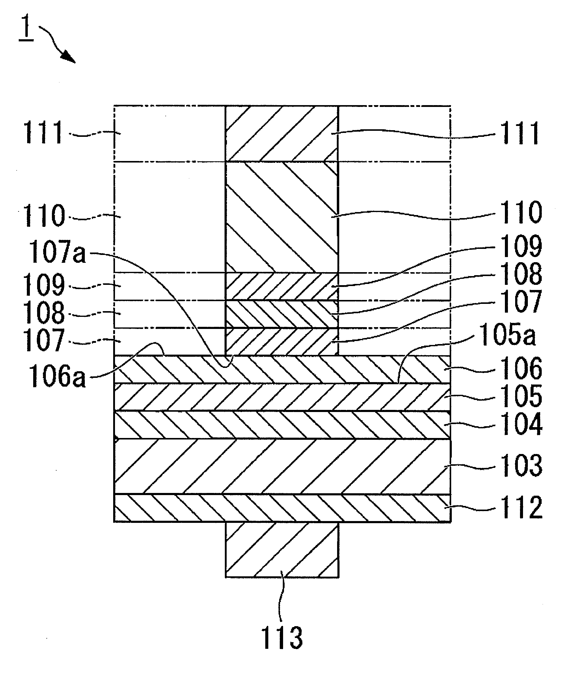
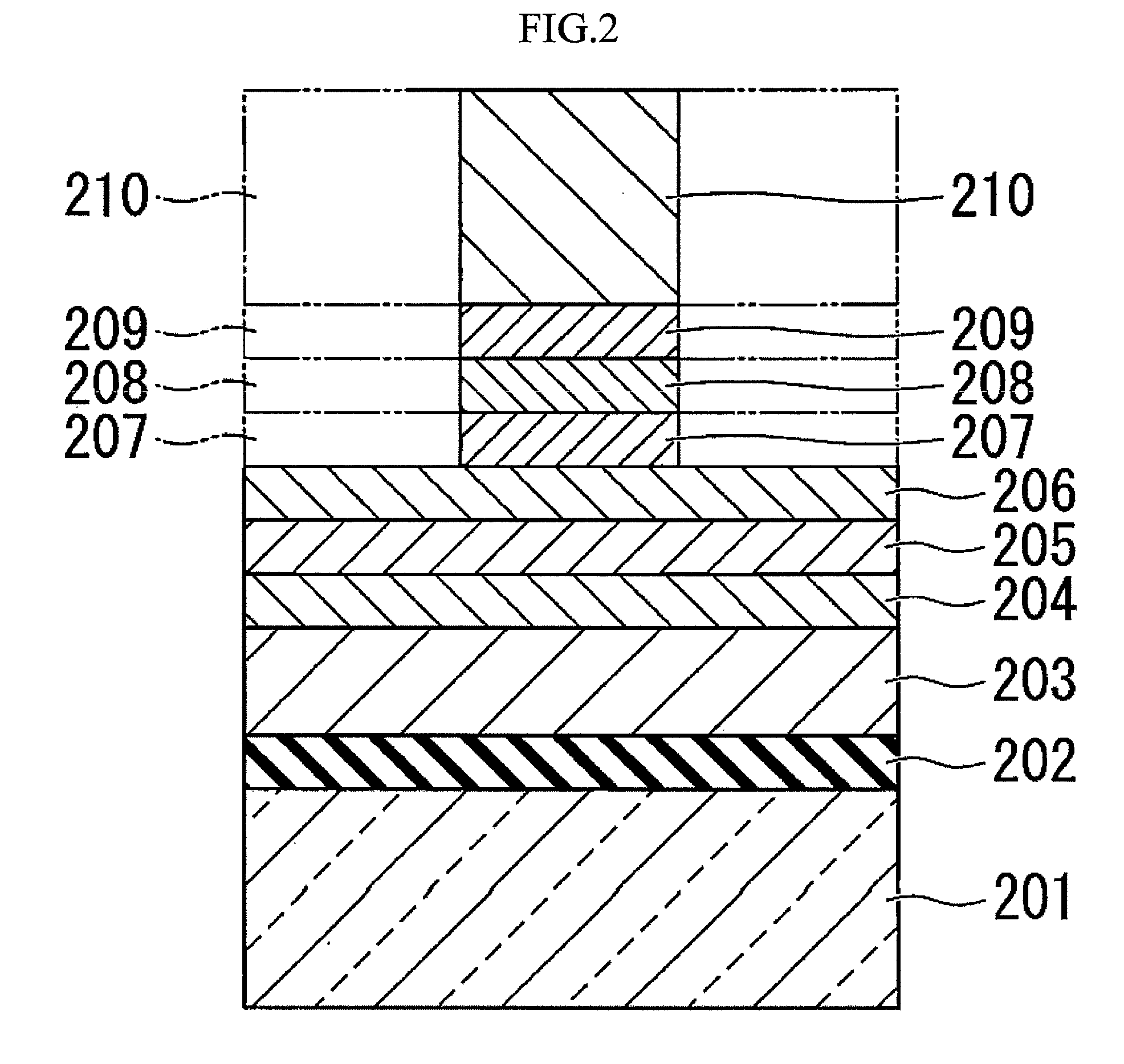
[0082]FIG. 1 to FIG. 4 show a nitride semiconductor light-emitting device of the present embodiment, and FIG. 1 is a cross-sectional view showing an example of a nitride semiconductor light-emitting device of the present invention, in which an n-type semiconductor layer, a light-emitting layer and a p-type semiconductor layer are formed, and on these layers, an ohmic layer, a reflection layer and a plating adhesion layer are formed, and on these layers, a plated metal plate is formed. FIG. 2 shows the method to produce a nitride semiconductor light-emitting device as an example. In the embodiment, the nitride semiconductor layer shown in FIG. 2 was formed before the formation of the structure of top and bottom placement of electrodes shown in FIG. 1. In addition, the two-dotted lines shown in FIG. 1 and FIG. 2 express the part of the cross shape from the top view formed by an ohmic layer, a reflection layer, a plating adhesion layer, a plated metal plate and a positive electrode (Po...

second embodiment

[0137]Another embodiment of a nitride semiconductor compound light-emitting device of the present invention is explained referring to figures.

[0138]FIG. 5 to FIG. 8 are figures explaining a nitride semiconductor light-emitting device of the present example, and FIG. 5 is a cross-sectional view showing an example of a nitride semiconductor light-emitting device of the present invention, in which an n-type semiconductor layer, a light-emitting layer and a p-type semiconductor layer are formed, and on these layers, an ohmic layer, a reflection layer and a plating adhesion layer are formed, and on these layers, a plated metal plate is formed. FIG. 6 is figure to explain the method to produce a nitride semiconductor light-emitting device as an example. In the embodiment, the nitride semiconductor layer shown in FIG. 6 was formed before the formation of the structure of top and bottom placement of electrodes shown in FIG. 5. In addition, the two-dotted lines shown in FIG. 5 show the part ...

example 1

[0215]In Example 1, a nitride semiconductor light-emitting device as shown in FIG. 1 which is a cross-sectional view, was produced.

[0216]Firstly, on a sapphire substrate, on the buffer layer 102 made of AlN having a thickness of 10 nm, a Si-doped n-type GaN contact layer having a thickness of 5 nm; an n-type In0.1Ga0.9N cladding layer having a thickness of 30 nm; a light-emitting layer having a multi-well structure in which a Si-doped n-type GaN barrier layer having a thickness of 30 nm and an In0.2G0.8N well layer having a thickness of 2.5 nm were stacked five times and then the barrier layer was stacked; a Mg-doped p-type Al0.07Ga0.93N cladding layer having a thickness of 50 nm; and a Mg-doped p-type GaN contact layer having a thickness of 150 nm were stacked successively.

[0217]On the p-type semiconductor layer 105, a transparent electrode made of an ITO film (SnO2: 10% by weight) having a thickness of 300 nm was deposited by an evaporation method, and was annealed for one hour at...


PUM

PropertyMeasurementUnit
thicknessaaaaaaaaaa
thicknessaaaaaaaaaa
refractive indexaaaaaaaaaa

Abstract

Disclosed is a semiconductor device which is improved in output power efficiency since reflection by the substrate is reduced. This semiconductor device is also excellent in strength characteristics of a supporting substrate. Also disclosed is a method for producing such a semiconductor device. Specifically disclosed is a nitride semiconductor device wherein at least an n-type semiconductor layer, a light-emitting layer, a p-type semiconductor layer, a metal film layer and a plated metal plate are sequentially stacked in this order on a substrate. This nitride semiconductor device is characterized in that the metal film layer and the plated metal plate are partially formed on the p-type semiconductor layer. Also disclosed is a nitride semiconductor device having a structure wherein at least an n-type semiconductor layer, a light-emitting layer, a p-type semiconductor layer, a metal film layer and a plated metal plate are sequentially stacked in this order, the device characterized in that the metal film layer and the plated metal plate are partially formed on the p-type semiconductor layer and a light-transmitting material layer is formed on the p-type semiconductor layer in a region where the metal film layer and the plated metal plate are not formed.

Description

TECHNICAL FIELD[0001]The present invention is related to a nitride semiconductor light-emitting device and a production method thereof.[0002]Priority is claimed on Japanese Patent Application No. 2005-272424, filed Sep. 20, 2005, and Japanese Patent Application No. 2005-272574, filed Sep. 20, 2005.BACKGROUND ART[0003]In recent years, gallium nitride (GaN)-based compound semiconductor light-emitting devices has attracted attention as short wavelength light-emitting devices. This gallium nitride based-compound semiconductor is formed using a method such as the metal-organic chemical vapor deposition method (MOCVD method) or the molecular beam epitaxial method (MBE method) on substrates of various oxides or group III to group V compounds starting with a sapphire single crystal.[0004]A sapphire single crystal substrate has a lattice constant which differs from the lattice constant of GaN by 10% or more. However, since a nitride semiconductor having excellent properties can be formed by ...

Claims


Application Information

Patent Timeline
Patent Type & Authority Applications(United States)
IPC IPC(8): H01L33/00H01L21/50H01L33/32H01L33/38H01L33/40H01L33/42
CPCH01L33/0079H01L33/32H01L33/42H01L33/405H01L33/38H01L33/0093
Inventor OSAWA, HIROSHIHODOTA, TAKASHI
Owner TOYODA GOSEI CO LTD
Why Eureka
Try Eureka