Photoelectric Conversion Device And Method For Manufacturing The Same

a technology photoelectric conversion device, which is applied in the field can solve the problems of low deposition rate, inconvenient use, and inferior productivity of photoelectric conversion device including microcrystalline silicon to those including amorphous silicon, and achieves the effects of reducing production costs, reducing production costs, and improving efficiency

Inactive Publication Date: 2009-12-03
SEMICON ENERGY LAB CO LTD
View PDF31 Cites 28 Cited by
  • Summary
  • Abstract
  • Description
  • Claims
  • Application Information

AI Technical Summary

Benefits of technology

[0043]According to an embodiment of the present invention, the semiconductor layer including in an amorphous structure, crystals penetrating between the impurity semiconductor layer having one conductivity type and the impurity semiconductor layer having a conductivity type opposite to the one conductivity type is formed as a photoelectric conversion layer. Therefore, the efficiency higher than that of a conventional photoelectric conversion device including amorphous silicon can be achieved. Further, with the semiconductor layer including in an amorphous structure, the crystals penetrating between the pair of impurity semiconductor layers bonded for forming an internal electric field, photodegradation or the like can be reduced and variation in characteristics can be suppressed as compared with a conventional photoelectric conversion device including amorphous silicon. The thickness of the photoelectric conversion layer can be the same or substantially the same as that of a photoelectric conversion device including amorphous silicon, and the productivity can be increased as compared with a conventional photoelectric conversion device including microcrystalline silicon. Thus, a photoelectric conversion device in which improvement is achieved in both characteristics and productivity can be provided.
[0044]Further, a plurality of cells is stacked, each of which has a semiconductor layer including in an amorphous structure, crystals penetrating between an impurity semiconductor layer having one conductivity type and an impurity semiconductor layer having a conductivity type opposite to the one conductivity type and which has a different proportion of the crystals in the semiconductor layer for each cell. Thus, the absorption wavelength range can be expanded to further increase the efficiency.
[0045]According to an embodiment of the present invention, a unit cell including a single crystal semiconductor layer as a photoelectric conversion layer and a unit cell including a non-single-crystal semiconductor layer formed over the unit cell including a single crystal semiconductor layer are provided. Thus, light in a wide wavelength range can be absorbed; therefore, an excellent photoelectric conversion characteristic can be obtained. When the upper unit cell includes a non-single-crystal semiconductor layer including in an amorphous structure, crystals penetrating between an impurity semiconductor layer having one conductivity type and an impurity semiconductor layer having a conductivity type opposite to the one conductivity type, higher efficiency than that of a conventional photoelectric conversion device including amorphous silicon can be achieved. Further, when the semiconductor layer including in an amorphous structure, crystals penetrating between the pair of impurity semiconductor layers bonded for forming an internal electric field is formed, photodegradation or the like can be reduced and variation in characteristics can be suppressed as compared with a conventional photoelectric conversion device including amorphous silicon. The thickness of the photoelectric conversion layer can be the same or substantially the same as that of a photoelectric conversion device including amorphous silicon, and the productivity can be increased as compared with a conventional photoelectric conversion device including microcrystalline silicon. Thus, a photoelectric conversion device in which improvement is achieved in both characteristics and productivity can be provided.

Problems solved by technology

However, they are not popular because the photoelectric conversion efficiency thereof is lower than that of bulk photoelectric conversion devices and there is still a problem of photodegradation called Staebler-Wronski effect.
However, since microcrystalline silicon is formed into films with the use of a semiconductor source gas typified by silane diluted with a large amount of hydrogen gas, there is a problem of low deposition rate.
For these reasons, photoelectric conversion devices including microcrystalline silicon are inferior in productivity to those including amorphous silicon.
In Patent Document 1, crystalline silicon (microcrystalline silicon is used in Patent Document 1) is formed into a film with uniform crystallinity and quality by the control of the pulse modulation in a high-frequency plasma CVD method; however, crystalline silicon is not practical because the deposition rate is low as compared with formation from amorphous silicon.
On the other hand, Patent Document 2 has improved the deposition rate but a silicon layer still needs to be several digit thicker than an amorphous silicon layer; therefore, the problem in productivity remains unsolved.
As a result, at present, the improvement of productivity and the improvement in characteristics, such as an increase in efficiency, cannot be achieved at the same time and the popularity of photoelectric conversion devices including silicon thin films comes short of that of bulk photoelectric conversion devices.
Moreover, the method as disclosed in Patent Document 3, i.e., the method in which a single crystal silicon substrate and another substrate are attached to each other using a paste for forming an electrode as an adhesive has problems in the degree of adhesion at the bonded portion and change in quality (decrease in adhesive strength) of the paste for forming the electrode which functions as the adhesive.

Method used


Image

  • Photoelectric Conversion Device And Method For Manufacturing The Same
  • Photoelectric Conversion Device And Method For Manufacturing The Same
  • Photoelectric Conversion Device And Method For Manufacturing The Same

Examples


embodiment 1

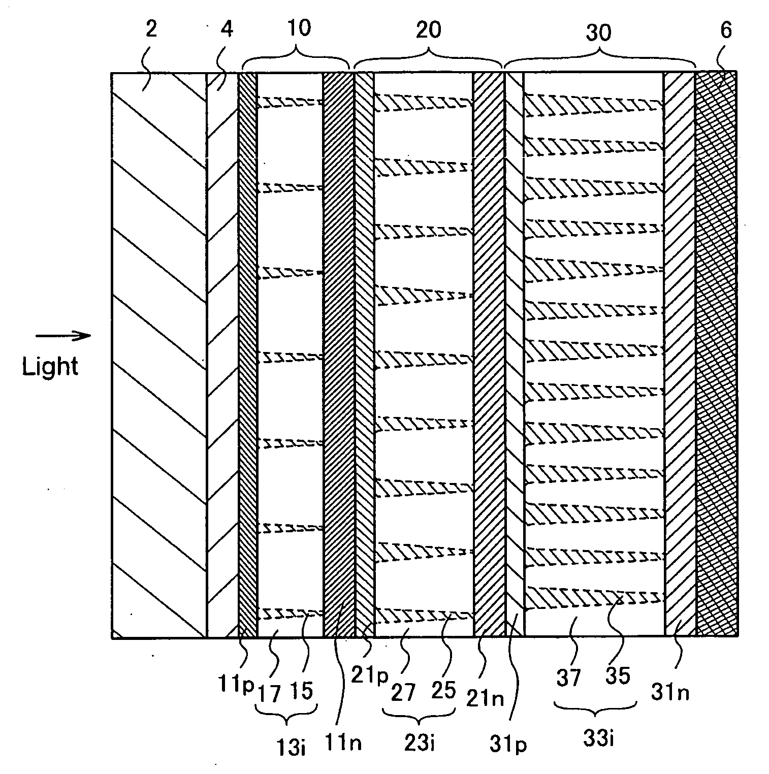
[0069]According to an embodiment of the present invention, a semiconductor layer which performs photoelectric conversion includes crystals in an amorphous structure and the crystals penetrate between a pair of impurity semiconductor layers bonded for forming an internal electric field. Embodiment 1 shows a photoelectric conversion device in which a plurality of unit cells is stacked. In the case of applying an embodiment of the present invention to a tandem or stack photoelectric conversion device, a semiconductor layer including in an amorphous structure, crystals penetrating between a pair of impurity semiconductor layers bonded for forming an internal electric field is used as a photoelectric conversion layer in at least one unit cell.

[0070]FIG. 1 is a schematic view of a unit cell according to an embodiment of the present invention. A unit cell according to an embodiment of the present invention has a structure in which a semiconductor layer 3i including in an amorphous structur...

embodiment 2

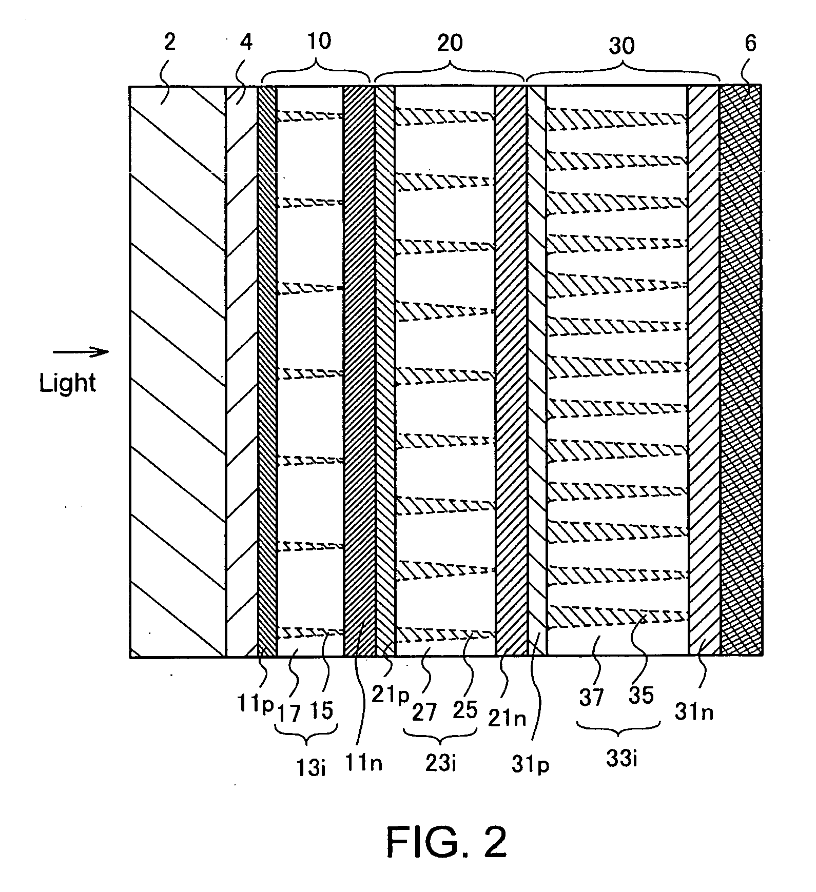
[0123]Embodiment 2 describes a photoelectric conversion device having a different structure from that described in Embodiment 1. Specifically, the number of stacked unit cells in the photoelectric conversion device of this example is different from that illustrated in FIG. 2.

[0124]FIG. 5A illustrates a single junction photoelectric conversion device including one unit cell. In this photoelectric conversion device which includes at least one semiconductor junction, a unit cell 40 is formed over a substrate 2 provided with a first electrode 4 and a second electrode 6 is formed over the unit cell 40. The unit cell 40 includes a stack of an impurity semiconductor layer 41p, which is a p-type semiconductor, a semiconductor layer 43i, which is an i-type semiconductor, and an impurity semiconductor layer 41n, which is an n-type semiconductor. In the semiconductor layer 43i, crystals 45 are provided discretely in an amorphous structure 47. The crystals 45 penetrate through the semiconductor...

embodiment 3

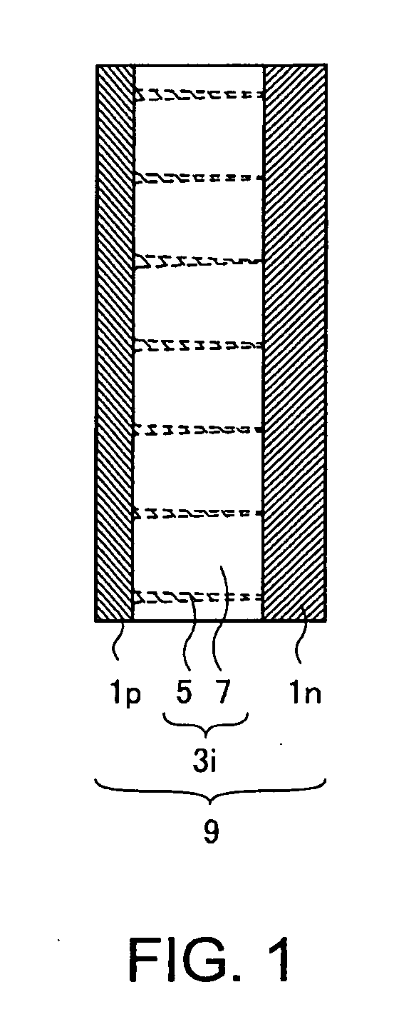
[0127]Embodiment 3 describes a photoelectric conversion device with a different structure from that in Embodiment 1 or 2. Specifically, an example is shown in which a junction portion between an impurity semiconductor layer having one conductivity type and an intrinsic semiconductor layer is provided with an impurity semiconductor layer having the same conductivity type as the one conductivity type and having lower impurity concentration than the impurity semiconductor layer having the one conductivity type.

[0128]Each of FIGS. 6A to 6C illustrates a stacked photoelectric conversion device in which three unit cells are formed. In FIG. 6A, a first unit cell 10, a second unit cell 20, a third unit cell 30, and a second electrode 6 are provided in that order over a substrate 2 provided with a first electrode 4. In the first unit cell 10, a first impurity semiconductor layer 11p, a first low-concentration impurity semiconductor layer 12p−, a first semiconductor layer 13i, and a second im...


PUM


Abstract

A photoelectric conversion device and a method for manufacturing the same are provided. The photoelectric conversion device includes a first semiconductor layer including a first impurity element over a substrate, a second semiconductor layer including an amorphous layer and a crystal over the first semiconductor layer, and a third semiconductor layer including a second impurity element over the second semiconductor layer. The crystal penetrates between the first semiconductor layer and the third semiconductor layer.

Description

BACKGROUND OF THE INVENTION[0001]1. Field of the Invention[0002]The present invention relates to a photoelectric conversion device including a semiconductor junction and a method for manufacturing the photoelectric conversion device.[0003]2. Description of the Related Art[0004]To deal with global environmental issues in recent years, the market has expanded for photoelectric conversion devices typified by solar cells such as residential photovoltaic systems. Bulk photoelectric conversion devices including single crystal silicon or polycrystalline silicon, which have high conversion efficiency, have already been put into practical use. The photoelectric conversion devices including single crystal or polycrystalline silicon are manufactured by cutting wafers out of large silicon ingots. However, since it takes a long time to manufacture large silicon ingots, the productivity is low. Further, since supply of raw materials of silicon itself is limited, the supply of silicon ingots is in...

Claims


Application Information

Patent Timeline
Patent Type & Authority Applications(United States)
IPC IPC(8): H01L31/0256H01L31/18H01L31/04H01L31/0725
CPCH01L31/03529H01L31/0725Y02E10/547H01L31/202H01L31/1804Y02E10/548Y02P70/50H01L31/04
Inventor YAMAZAKI, SHUNPEI
Owner SEMICON ENERGY LAB CO LTD
Why Eureka
Try Eureka