

Apparatus for inspecting a substrate, a method of inspecting a substrate, a scanning electron microscope, and a method of producing an image using a scanning electron microscope
a scanning electron microscope and substrate technology, applied in the direction of instruments, mass spectrometers, beam deviation/focusing by electric/magnetic means, etc., can solve the problems of affecting the quality of sem images, and affecting the inspection accuracy of substrates, etc., to achieve excellent substrate inspection, high-quality sem images, and sensitive defect detection capabilities
- Summary
- Abstract
- Description
- Claims
- Application Information
AI Technical Summary
Benefits of technology
Problems solved by technology
Method used
Image

Examples
first embodiment
(1) First Embodiment
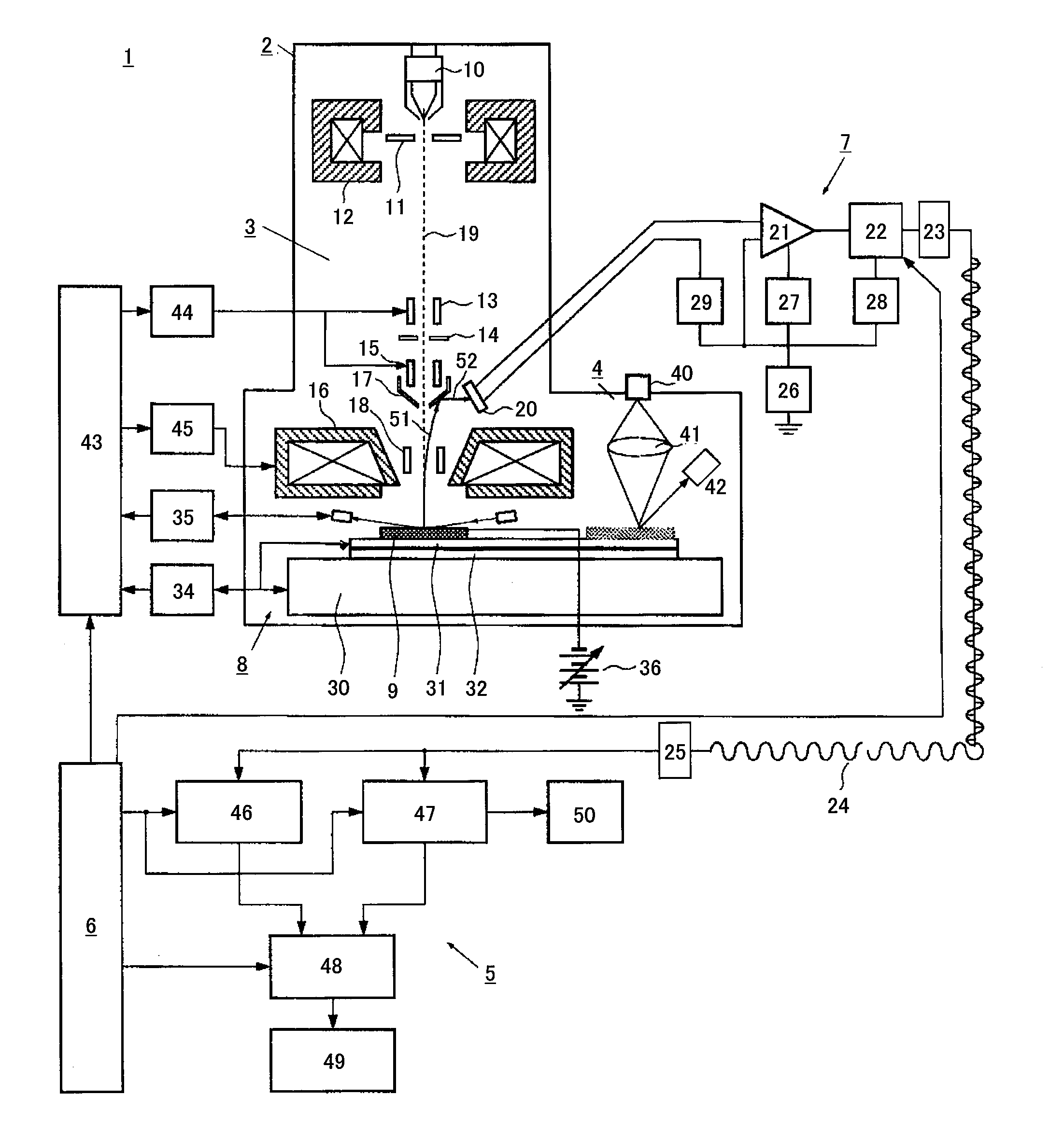
[0062]FIG. 1 is a vertical sectional view schematically showing the configuration of an SEM-type visual inspection apparatus 1 that is an example of an inspection apparatus using a scanning electron microscope to which the present invention is applied.
[0063]An SEM-type visual inspection apparatus 1 includes an inspection chamber 2 the interior of which is evacuated, a preliminary chamber (not shown in the present embodiment) from which a substrate 9 is conveyed into the inspection chamber 2, an image processing section 5, a control section 6, and a secondary electron detecting section 7. The preliminary chamber is configured to be able to be evacuated independently of the inspection chamber 2. Roughly speaking, an electronic optical system 3, a substrate chamber 8, and an optical microscope section 4 are provided in the inspection chamber 2.
[0064]The electronic optical system 3 is composed of an electron gun 10, an electron bean lead-out electrode 11, a condenser...
second embodiment
(2) Second Embodiment
[0095]In a second embodiment, description will be given of the use of a height measuring instrument based on a scheme different from that in the first embodiment, for example, laser interferometer-type shape measuring instrument or an electrostatic capacitance-type displacement meter. The remaining part of the configuration of the second embodiment is similar to that of the first embodiment and will thus not be described.
[0096]FIG. 7 is a diagram schematically showing the configuration of a laser interferometer-type shape measuring instrument (Fizeau interferometer) 250. With reference to FIG. 7, the principle of the height measurement will be described. In the laser interferometer-type shape measuring instrument 250, a laser beam from a laser head 251 passes through a divergence lens 252, a beam splitter 253, and a collimator lens 254. The laser beam then becomes parallel light, which reaches a precisely polished planar glass plate called a reference plate 255....
third embodiment
(4) Third Embodiment
[0112]FIG. 10 is a diagram showing the general configuration of an SEM-type inspection apparatus.
[0113]The inspection apparatus as a whole is composed of an electronic optical system 1010, a table control system 1020, a detection system 1030, an image processing system 1040, a height detecting system 1050, a control system 1060, a secondary storage device 1121, and a computer 1123. The inspection apparatus is connected to a network 1138.
[0114]The electronic optical system 1010 includes an electron gun 1101, condenser lenses 1102 and 1103, polarizers 1105 and 1106, an objective lens 1107, a surface field control plate 1132, and a shield electrode 1133.
[0115]The table control system 1020 includes a substrate holder 1134, an XY stage 1117, and a stage position measuring section 1104 such as a laser length measuring instrument.
[0116]The detection system 1030 includes an ExB polarizer 1110, an electron detector 1111, and an A / D converter 1112.
[0117]The image processin...
PUM
 Abstract
Description
Claims
Application Information