Selective area epitaxy growth method and structure

a growth method and selective area technology, applied in the direction of crystal growth process, nanoinformatics, polycrystalline material growth, etc., can solve the problems of reducing material quality, poor crystal quality, and difficult growth of quality in-containing layers such as ingan with sufficient content to achieve emission wavelengths beyond 400 nm to the blue, green, yellow and red regime, etc., to achieve high incorporation, high brightness, and reinforce viability and promise

Inactive Publication Date: 2009-12-17
SORAA +1
View PDF102 Cites 250 Cited by
  • Summary
  • Abstract
  • Description
  • Claims
  • Application Information

AI Technical Summary

Benefits of technology

[0010]Here we propose to use selective area epitaxy (SAE) to achieve increased-In-content InGaN layers without changing the MOCVD reactor growth conditions. That is, for the same growth pressure, temperature, and partial pressures of the In and Ga precursors, the solid composition of the InGaN film will possess higher In levels. This technique will enable increased temperature growth conditions to avoid the low temperatures conditions commonly used for increased-In-content InGaN) that are known to degrade crystal quality. In SAE, a dielectric (SiO2, SixNy, etc) mask is deposited on the substrate surface, lithographically patterned, and then etched such that various geometries of exposed semiconductor are realized. For laser diode fabrication the geometry of the unmasked area is often a long (100s of microns) narrow (1-5 microns) stripe. When subjected to epitaxial growth in an MOCVD reactor where the group-III precursors have a high surface and gas phase mobility, growth initiation can be prevented in the masked areas. A growth rate enhancement is observed in the unmasked areas adjacent to the dielectric mask from the increased concentration of the growth rate limiting group-III (In and Ga) adatoms within these areas. The lack of depletion of the group-III precursor molecules in the gas phase over the masked regions coupled with the high surface mobility of the group-III adatoms on the masked areas leads to an increased concentration of the group-III adatoms present in the growth area adjacent to the dielectric mask boundary. A key aspect of our invention is that the difference between the diffusion properties of the In and Ga precursors leads to In-enrichment in the InGaN layer adjacent to the dielectric mask. The metalorganic compounds trimethylindium (TMIn) and trimethylgallium (TMGa) are often used as the source material for In and Ga, respectively. Other source materials include triethylgallium, commonly known as TEGa, among others. The TMIn molecule decomposes more efficiently than TMGa in the high temperature MOCVD growth conditions, leading to a reduced average size of the In containing metalorganic molecules. Since the gas-phase diffusion coefficient increases with reduced molecule size, the In precursors will have a higher diffusivity and will therefore more readily arrive in the growth areas. The result is a relatively higher In content in the In and Ga containing layer (i.e. InGaN) adjacent to the dielectric mask for a given set of reactor conditions. The kinetics of SAE are a well understood phenomenon in traditional alloys such as InGaAs and InGaAsP [2]. Literature reports similar phenomenon on polar GaN, where researchers have grown InGaN quantum dots and multi-color LEDs using SAE.
[0011]According to an embodiment of the present invention, SAE is used to overcome the formidable challenge of realizing high-In-content InGaN quantum wells for the fabrication of high-efficiency laser diodes and LEDs with extended wavelengths beyond 450 nm into the blue, green, yellow and red regimes. The implementation of SAE will facilitate increased In incorporation in the In containing layer such as InGaN quantum wells adjacent to the masked region under identical growth conditions. This technique will be executed on nonpolar and / or semipolar GaN substrates to facilitate high-efficiency long-wavelength laser diodes and LEDs. Lasers and LEDs fabricated on conventional polar (c-plane) GaN suffer from internal piezoelectric and spontaneous polarization fields that intrinsically reduce the radiative recombination efficiency of electron-hole pairs and limit the device performance [3,4]. Early demonstrations of laser diodes fabricated on nonpolar (m-plane) GaN substrates operating at 405 nm and 451.8 nm show great promise for enhanced device performance [5, 6]. Furthermore, high-power green (516 nm) light emitting diodes (LED) fabricated on semipolar substrates indicate a natural tendency for increased In-incorporation on these crystallographic planes [7]. By coupling this enhanced In-incorporation behavior with minimized internal piezoelectric and spontaneous fields on semipolar substrates with our proposed SAE method for increased In-incorporation, our invention will enable the fabrication of high-efficiency blue, green, yellow and red emitting laser diodes and LEDs.
[0012]Laser diodes will be fabricated by patterning a dielectric mask either directly on the nonpolar / semipolar substrate or on an n-doped layer grown on the said substrates to form narrow stripes of unmasked growth area. The wafers will then be subjected to MOCVD growth where growth will initiate with an n-type GaN cladding layer, followed by the active region containing In containing quantum wells such as InGaN. The growth of the InGaN quantum wells in these narrow unmasked stripe areas will result in high-In-content quantum wells based on the SAE kinetics discussed above, pushing the emission wavelength to values required for blue, green, yellow and red emission. After deposition of the active region layers, the growth can be continued to deposit the p-GaN upper cladding layer or the growth can be interrupted. In the latter case, the sample would be removed from the reactor, the dielectric mask selectively etched, and the sample would be subjected to a regrowth for the definition of the p-cladding layer to realize a buried stripe laser structure. In the former case, where the p-cladding is defined in the same growth as the active region, surface ridge laser architectures could be easily fabricated from the resulting epitaxial structure.
[0016]Other benefits are achieved over conventional techniques. For example, the present method and device achieves high brightness and high resolution lighting technologies that require blue, green, yellow or red contributions such as high resolution red-green-blue displays, communications in polymer-based fibers, or solid-state lighting based on red-greenblue or blue-yellow laser diodes and LEDs. In a specific embodiment, the present invention provides improved crystal quality, highly efficient laser diodes and LEDs on nonpolar / semipolar GaN will enable laser and LED emission in the blue, green, yellow and red bands, allowing the realization of true color displays based on red-green-blue or blue-yellow laser diodes. In a preferred embodiment, the absence of polarization fields in the quantum wells on the substrates along with the increased growth temperatures enabled by SAE will facilitate high efficiency device operation. Thus, this technology would allow for the improvement of existing devices such as 405 nm lasers used in HD-DVD and Sony BlueRay™ along with completely new technologies demanding blue, green, yellow and red emission and low power consumption. Additionally, depending upon the embodiment, the indium concentration is provided preferably within a center region of the growth region and more preferably includes edges regions of the growth region as well. Such indium concentration is generally greater than the use of conventional techniques having larger spatial areas of growth according to a specific embodiment. These and other benefits are described throughout the present specification and more particularly below.

Problems solved by technology

The growth of quality In-containing layers such as InGaN with sufficient In content to achieve emission wavelengths beyond 400 nm to the blue, green, yellow and red regime has historically been difficult [1].
This difficulty manifests itself with a reduction of material quality as the MOCVD reactor growth conditions are changed to facilitate increased-In-content InGaN.
More specifically, the reduced growth temperatures required to prevent In evaporation are known to lead to poor crystal quality.
The microstructural nature of the degraded material is a contentious topic as some research groups attribute it to compositional In fluctuations, while others claim it is a result of localized strain.
In any case, the poor material quality has prevented the demonstration of an efficient laser diode at wavelengths beyond 400 nm.
Lasers and LEDs fabricated on conventional polar (c-plane) GaN suffer from internal piezoelectric and spontaneous polarization fields that intrinsically reduce the radiative recombination efficiency of electron-hole pairs and limit the device performance [3,4].

Method used


Image

  • Selective area epitaxy growth method and structure
  • Selective area epitaxy growth method and structure
  • Selective area epitaxy growth method and structure

Examples


Embodiment Construction

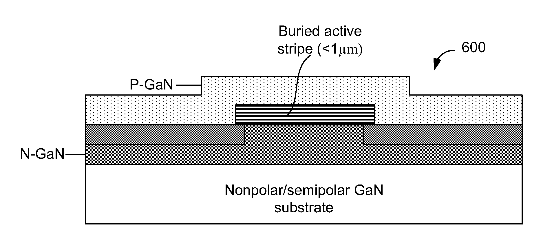
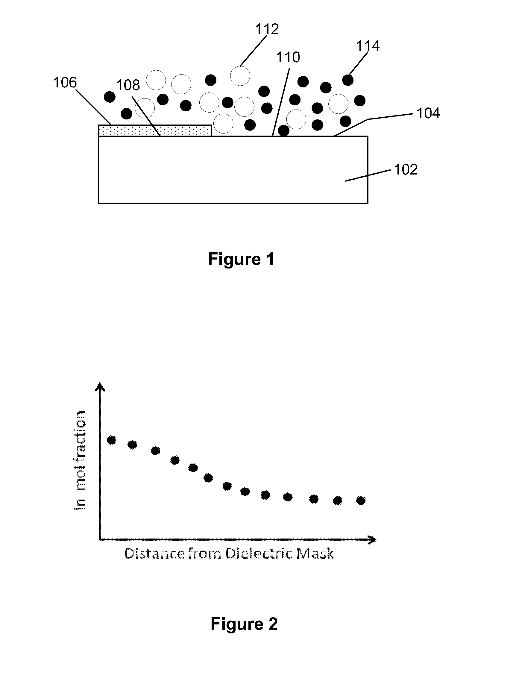
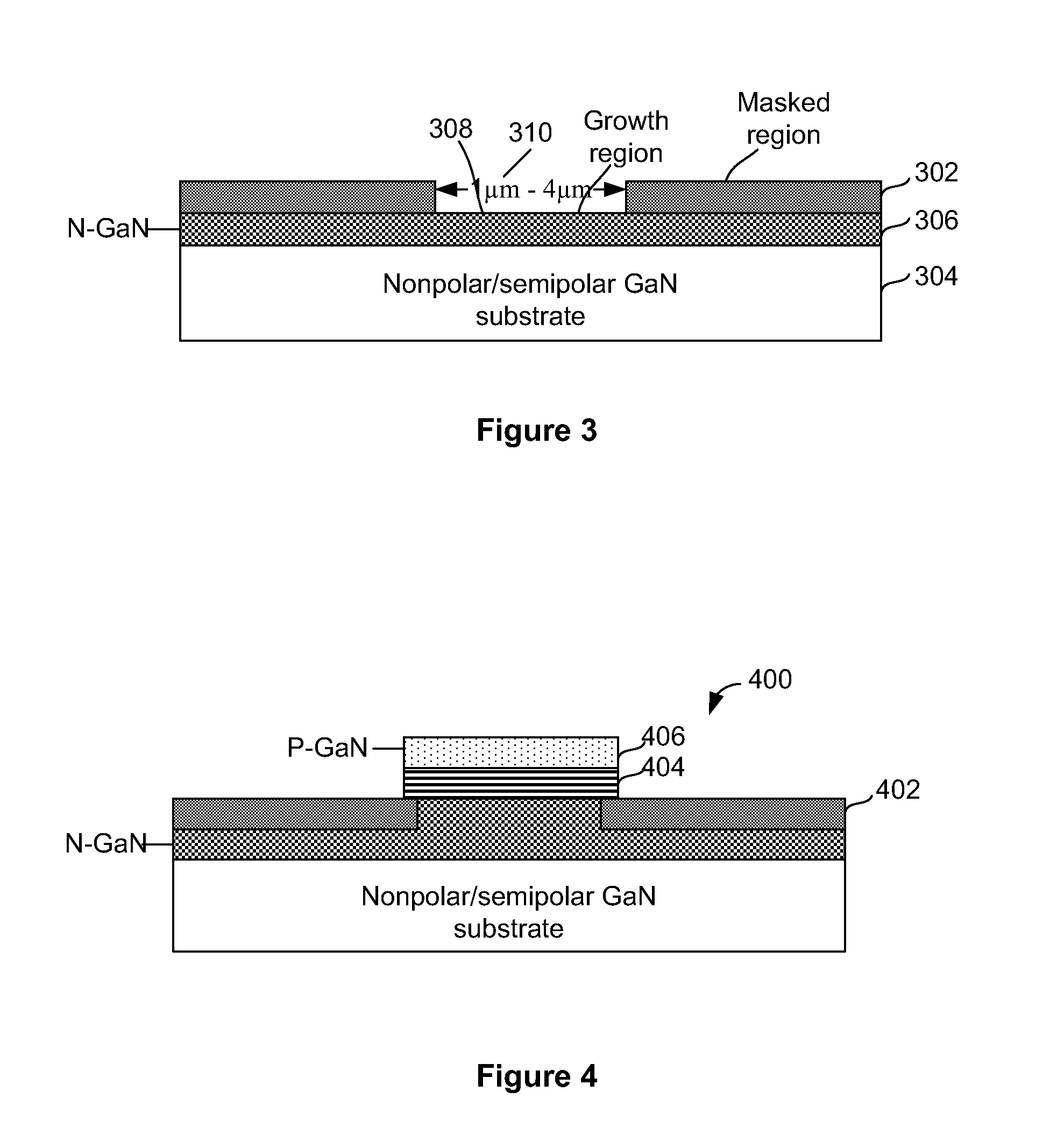
[0025]According to embodiment of the present invention, techniques related generally to optical devices are provided. More particularly, embodiment according to the present invention provides a method and device for emitting electromagnetic radiation using non-polar or semipolar gallium containing substrates such as GaN, MN, InN, InGaN, AlGaN, and AlInGaN, and others. Merely by way of example, the invention can be applied to optical devices, lasers, light emitting diodes, solar cells, photoelectrochemical water splitting and hydrogen generation, photodetectors, integrated circuits, and transistors, among other devices.

[0026]The present invention is directed to generate high efficiency GaN-based light emitting devices operating at wavelengths beyond 400 nm for blue, green, yellow and red emission. The proposed device will be used as an optical source for various commercial, industrial, or scientific applications. These structures are expected to find utility in existing applications ...


PUM

PropertyMeasurementUnit
mole fractionaaaaaaaaaa

Abstract

A gallium containing crystalline material. The material comprises a bulk semi-polar gallium indium containing crystalline material having a thickness of about 20 nanometers to about 1000 nanometers. The material includes a spatial width dimension of no greater than about 10 microns characterizing the thickness of the bulk semi-polar gallium indium containing crystalline material. The material includes a photoluminescent characteristic of the crystalline material having a first wavelength, which is at least five nanometers greater than a second wavelength, which is derived from an indium gallium containing crystalline material grown on a growth region of greater than about 15 microns.

Description

CROSS-REFERENCES TO RELATED APPLICATIONS[0001]This application claims priority to U.S. Provisional Application No. 61 / 061,521, filed Jun. 13, 2008, entitled “SELECTIVE AREA EPITAXY GROWTH METHOD AND STRUCTURE,” by inventors James W. Raring, Daniel F. Feezell, and Shuji Nakamura commonly assigned, and incorporated by reference herein for all purposes.BACKGROUND OF THE INVENTION[0002]The present invention is directed to optical devices and related methods. More particularly, the present invention provides a method and device for emitting electromagnetic radiation using non-polar or semipolar gallium containing substrates such as GaN, MN, InN, InGaN, AlGaN, and AlInGaN, and others. Merely by way of example, the invention can be applied to optical devices, lasers, light emitting diodes, solar cells, photoelectrochemical water splitting and hydrogen generation, photodetectors, integrated circuits, and transistors, among other devices.[0003]In the late 1800's, Thomas Edison invented the l...

Claims


Application Information

Patent Timeline
Patent Type & Authority Applications(United States)
IPC IPC(8): H01L33/00H01L29/12C30B25/02H01L33/06H01L33/08H01L33/16
CPCB82Y10/00C30B25/02C30B25/04C30B29/403H01L33/16H01L29/2003H01L33/0079H01L33/06H01L33/08H01L29/122H01L33/0093
Inventor RARING, JAMES W.FEEZELL, DANIEL F.NAKAMURA, SHUJI
Owner SORAA
Why Eureka
Try Eureka