

Strained-silicon-on-insulator single-and double-gate mosfet and method for forming the same
a strain-silicon-on-insulator and mosfet technology, applied in the field of strained-silicon-on-insulator mosfet, can solve the problems of limiting the final portfolio one can create, the epi-layer of relatively thick sige is needed, and the method typically cannot deal with this type of dependence, etc., to achieve enhanced n-type dopant diffusion and eliminate the problem of sige as the device substrate.
- Summary
- Abstract
- Description
- Claims
- Application Information
AI Technical Summary
Benefits of technology
Problems solved by technology
Method used
Image

Examples
second embodiment
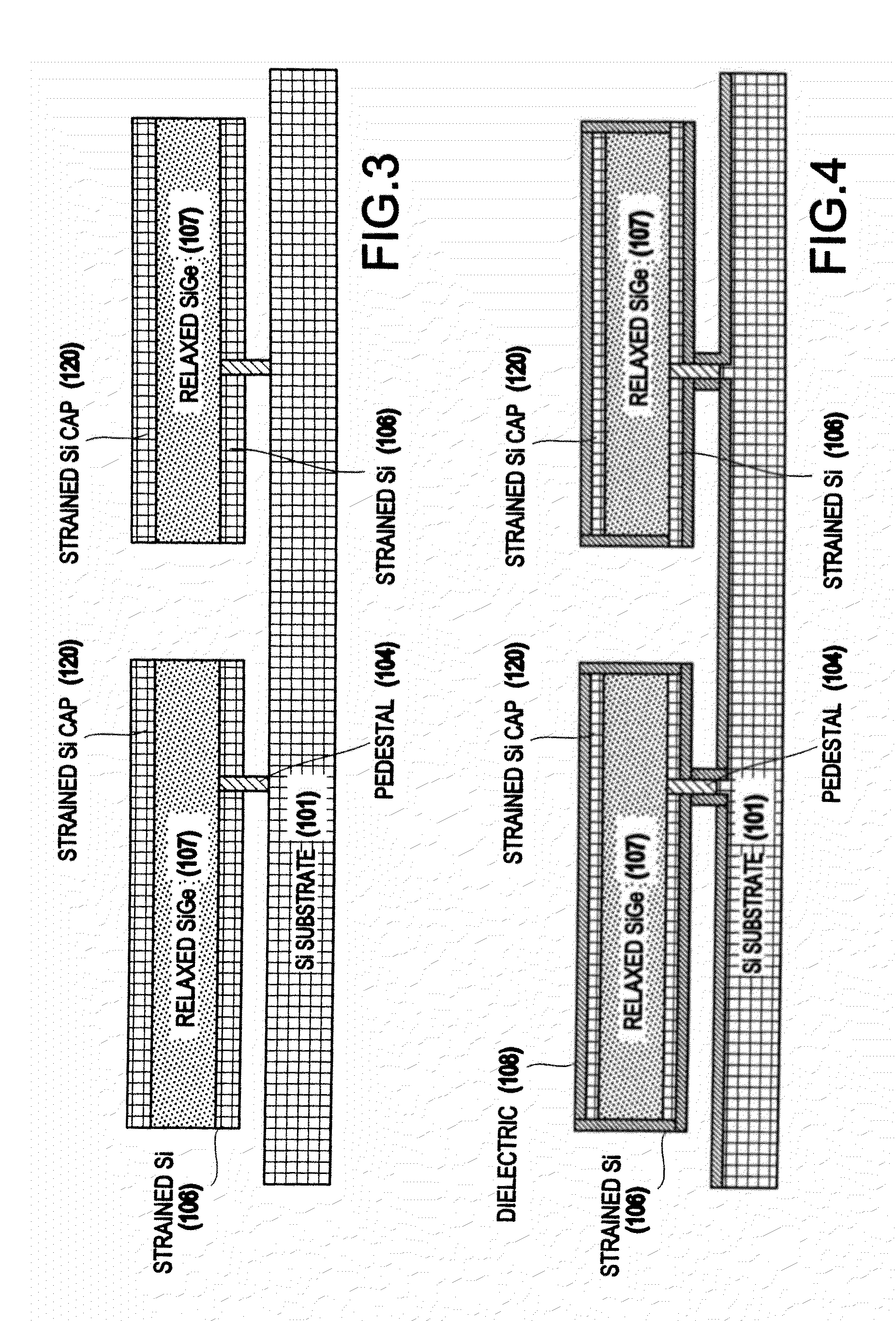
[0102]Turning now to FIG. 11 and to a different structure, it is noted that bowing occurs since the free-standing structure includes a bilayer of two mismatched materials such as SiGe over silicon. The bowing can be prevented by sandwiching the SiGe 107 film between two silicon films (106 and 120) of equal thicknesses, as was discussed above and shown in FIGS. 2-6. The sandwiched SiGe film 107 does not bow since the silicon layer 106 balances the silicon cap layer 120.
[0103]Hence, whereas before in FIGS. 2-6, a sandwich layer was shown of relaxed SiGe with strained silicon on first and second sides (e.g., top and bottom), in FIGS. 11-12, a first side (e.g., the top) of the strained silicon has been removed.
[0104]However, the use of a cap layer 120 decreases the degree of strain relaxation in SiGe film 107, since the total silicon film thickness, t.sub.Si, is twice as thick compared with a bilayer structure (e.g., SiGe over silicon without a silicon cap).
[0105]Thus, it is possible to...
third embodiment
[0108]It is noted that the fabrication of a free-standing structure according to the present invention does not necessarily require the use of a SOI wafer, but can also be achieved with a bulk silicon wafer as the starting wafer. This allows the integration of mixed complementary metal oxide semiconductor (CMOS) technologies (e.g., bulk Si CMOS with SSOI CMOS, etc.).
[0109]Referring now to FIGS. 13-20, a bulk silicon substrate 121 is implanted with a p-type dopant such as boron. The implant forms a buried p-doped layer 122 which is capped by an undoped silicon layer 123, as shown in FIG. 13. Alternatively, the p-doped layer 22 can be realized by in-situ doped epitaxial growth of p-type silicon followed by an epitaxial growth of undoped silicon to form the cap layer 123.
[0110]The pedestal location is defined by a masked implant that forms a localized pillar of doped silicon 122A. The structure is then annealed to activate the dopants. The pedestal can also be formed by the “drill and ...
fourth embodiment
[0120]FIGS. 21-25 describe an embodiment in which a free-standing silicon film 136 is strained by the deposition of a straining material 137. It is assumed in this embodiment a BOX 132 and SOI 133 is used. Of course, a bulk silicon substrate could be used instead, as demonstrated above.
[0121]As shown in FIGS. 21-22, a free-standing silicon film 136 is formed by first forming a pedestal 134, patterning the SOI film 133, and etching the BOX 132.
[0122]Then, as shown in FIG. 23, a straining material 137 is deposited over the free-standing silicon and over the silicon substrate 131.
[0123]An exemplary feature of this embodiment is that the straining material can be many materials (e.g., SiGe, or a material other than SiGe such as a layer of silicon nitride, etc.). Hence, the straining material 37 can be deposited as single-crystal by epitaxy, or it can be deposited as an amorphous or poly-crystalline material. Examples of single-crystal materials are SiGe, SiC or metal-oxides such as Al2O...
PUM
 Abstract
Description
Claims
Application Information