Semiconductor device and manufacturing method thereof

a technology of semiconductor devices and manufacturing methods, applied in the direction of solid-state devices, resistive material coatings, printed circuit assembling, etc., can solve the problems of resin-impregnated fibrous-body composite substrates that cannot function as sealing materials, air tightness cannot be maintained, and strength of resin-impregnated fibrous-body composite substrates can be decreased, so as to achieve mechanical strength and maintain air tightness, the effect of maintaining mechanical strength

Inactive Publication Date: 2009-12-24
SEMICON ENERGY LAB CO LTD
View PDF28 Cites 40 Cited by
  • Summary
  • Abstract
  • Description
  • Claims
  • Application Information

AI Technical Summary

Benefits of technology

[0015]According to one embodiment of the invention disclosed in this specification, even when a through wiring is provided in a wiring substrate which uses a resin-impregnated fibrous-body composite material, the wiring substrate is strong and can maintain mechanical strength.
[0016]Acco

Problems solved by technology

However, formation of a through hole in a composite substrate, such as a prepreg, in which a fibrous body is impregnated with a resin (hereinafter also referred to as a resin-impregnated fibrous-body composite substrate) damages a sheet-like fibrous body as a reinforcing material, whereby the strength of the resin-impregnated fibrous-body composite substrate is decreased.
In the case of using the resin-impregnated fibrous-body co

Method used


Image

  • Semiconductor device and manufacturing method thereof
  • Semiconductor device and manufacturing method thereof
  • Semiconductor device and manufacturing method thereof

Examples


embodiment 1

[0031]In Embodiment 1, the structure of a wiring substrate and a manufacturing method thereof will be described with reference to FIGS. 1A and 1B and FIGS. 2A to 2C.

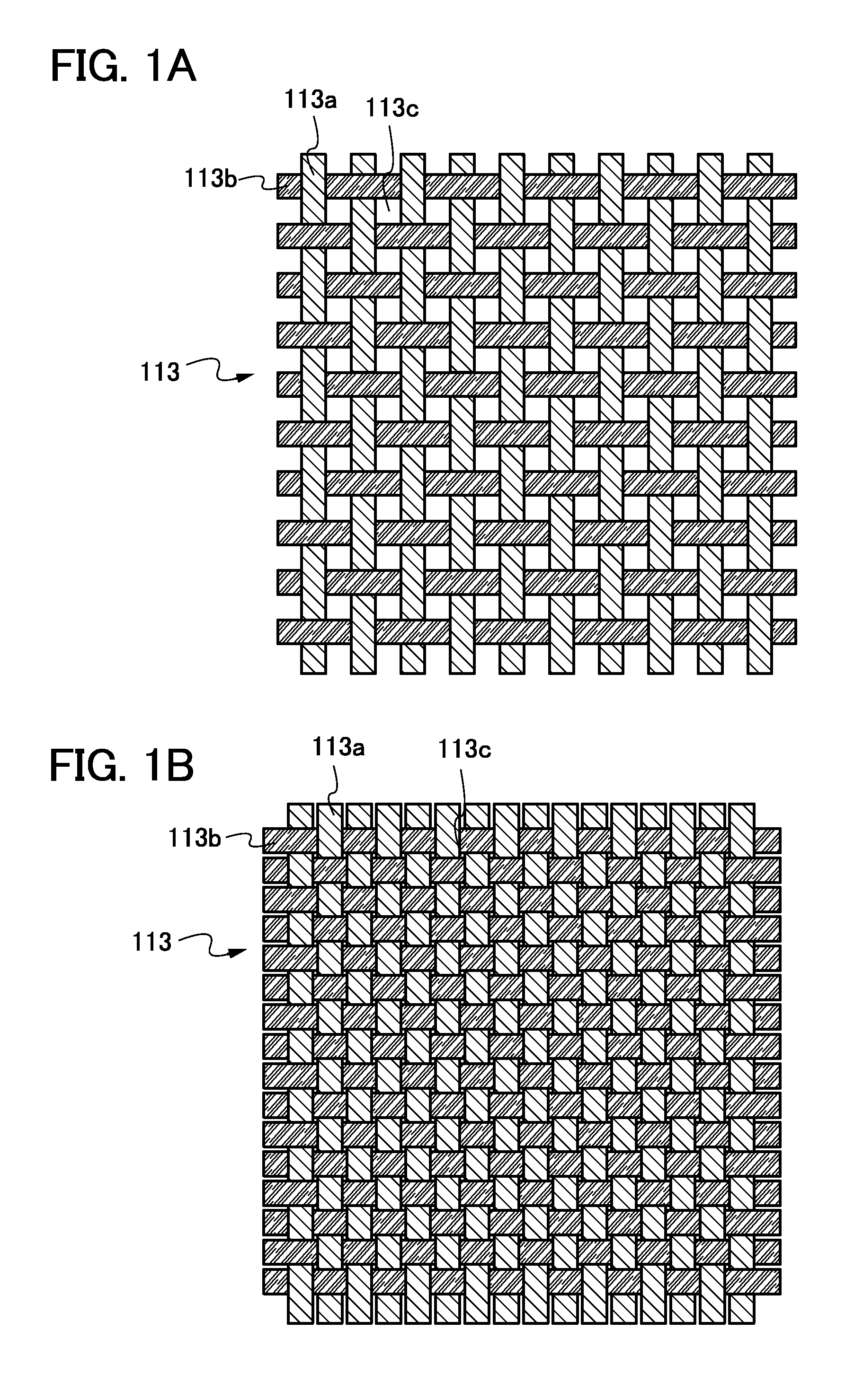
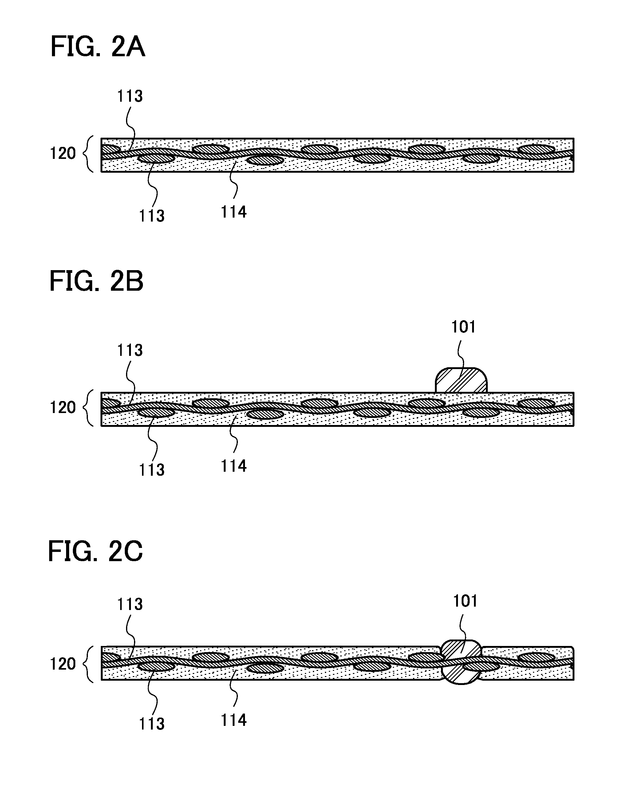
[0032]FIGS. 1A and 1B are each a top view of a sheet-like fibrous body 113 which is a fabric woven using yarn bundles for warp yarns and weft yarns. FIG. 2A is a cross-sectional view of a structure body 120 in which the sheet-like fibrous body 113 is impregnated with an organic resin 114.

[0033]The sheet-like fibrous body 113 is a woven fabric or a nonwoven fabric of an organic compound or an inorganic compound. Further, as the sheet-like fibrous body 113, a high-strength fiber of an organic compound or an inorganic compound may be used.

[0034]The sheet-like fibrous body 113 may be formed using a woven fabric which is woven using bundles of fibers (single yarn) (hereinafter, referred to as yarn bundles) for warp yarns and weft yarns, or a nonwoven fabric obtained by stacking yarn bundles of plural kinds of fibers in a rand...

embodiment 2

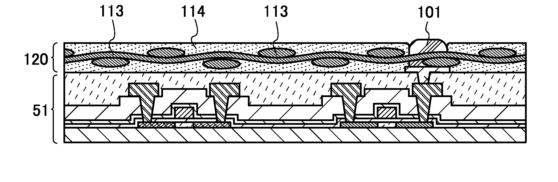
[0050]In Embodiment 2, a structure of a semiconductor device using a resin-impregnated fibrous-body composite substrate which is provided with a through wiring, and a manufacturing method thereof will be described with reference to FIGS. 3A to 3D, FIGS. 4A to 4E, FIGS. 5A to 5D, FIGS. 6A to 6E, and FIGS. 9A and 9B.

[0051]FIGS. 3A to 3D are cross-sectional views of element layers.

[0052]First, an element layer 51 illustrated in FIG. 3A has the same structure as those of FIGS. 4A to 4E, FIGS. 5A to 5D, FIGS. 6A to 6E, and FIGS. 9A and 9B. In FIGS. 3B to 3D, the same components as those in FIG. 3A are denoted by the same reference numerals.

[0053]The element layer 51 includes a thin film transistor 52a, a thin film transistor 52b, an insulating film 65, an insulating film 66, and an insulating film 67 over an insulating layer 56. The thin film transistor 52a includes a semiconductor layer including impurity regions 53a which are a source region and a drain region and a channel formation r...

embodiment 3

[0120]In Embodiment 3, examples in which Embodiment 1 and Embodiment 2 are applied to an external antenna of an RFID tag or connection with the external antenna will be described with reference to FIGS. 10A to 10C and FIGS. 11A to 11G.

[0121]First, FIG. 10A illustrates a chip of an RFID tag. The chip is formed over a substrate 201 from which the chip can be separated, and includes a semiconductor circuit portion 202, an electrode pad 203, and a conductive resin 204. The semiconductor circuit portion 202 may be formed using the structure illustrated in FIG. 3D in Embodiment 2 or the like. For the substrate 201, a flexible substrate or a glass substrate may be used. Any conductive resin that includes any of copper (Cu), silver (Ag), nickel (Ni), gold (Au), platinum (Pt), palladium (Pd), tantalum (Ta), molybdenum (Mo), titanium (Ti), and tin (Sn) may be used as the conductive resin 204.

[0122]FIG. 10B illustrates an RFID tag in which the chip illustrated in FIG. 10A is connected to an ex...


PUM

PropertyMeasurementUnit
Electrical conductoraaaaaaaaaa

Abstract

To form a conductive region in a prepreg without opening a through hole in a fibrous body. A wiring substrate is provided, including: an organic resin layer and a fibrous body, wherein the fibrous body is impregnated with the organic resin layer; and a wiring with which the fibrous body is impregnated and which is formed by dissolving the organic resin layer. The wiring is exposed on both surfaces of the organic resin layer and penetrates the fibrous body so that the fibrous body is positioned in the through wiring. Further, a semiconductor device is provided by adhering an integrated circuit chip having a bump to the wiring substrate so that the bump is in contact with the wiring.

Description

BACKGROUND OF THE INVENTION[0001]1. Field of the Invention[0002]The present invention relates to a wiring substrate which electrically and / or mechanically connects a semiconductor integrated circuit or a circuit substrate, and a semiconductor device using the wiring substrate.[0003]2. Description of the Related Art[0004]A prepreg in which a sheet-like fibrous body as a reinforcing material is impregnated with a thermosetting resin and the thermosetting resin is made in a semi-cured state has been used as a member of a circuit substrate and the like.[0005]For example, a prepreg formed by opening a through hole in a predetermined position and filling the through hole with a conductive paste to become a conductor through an insulating layer by hot pressing is known in which a conductor passes and which is (see Patent Document 1: Japanese Published Patent Application No. 2007-091822). In this case, the through hole is opened in the prepreg by a laser, a drill, a punching machine, or the...

Claims


Application Information

Patent Timeline
IPC IPC(8): H05K1/03H05K1/16B05D5/12H01L21/50
CPCG06K19/07745Y10T29/49126G06K19/07749G06K19/0775H01L21/6835H01L23/145H01L23/49827H01L23/5389H01L27/1266H01L2221/6835H01L2924/12044H01L2924/14H01L2924/19041H01L2924/3025H05K1/0366H05K3/002H05K3/4069H05K3/4644H05K2203/1163H01L2924/0002G06K19/07747Y10T29/49169H01L27/1218H01L2924/00
Inventor HATANO, KAORUCHIDA, AKIHIRONAGATA, TAKAAKISAKAKURA, MASAYUKI
Owner SEMICON ENERGY LAB CO LTD
Why Eureka
Try Eureka