Method for Manufacturing Memory Element
a memory element and manufacturing method technology, applied in the field of memory elements, can solve the problems of high unit price of the rfid tag, inability to rewrite the memory element, and disturb the spread of merchandise and cargo management systems, etc., and achieve the effect of convenient and inexpensive manufacturing, convenient and fast delivery, and convenient and fast delivery
- Summary
- Abstract
- Description
- Claims
- Application Information
AI Technical Summary
Benefits of technology
Problems solved by technology
Method used
Image

Examples
embodiment 1
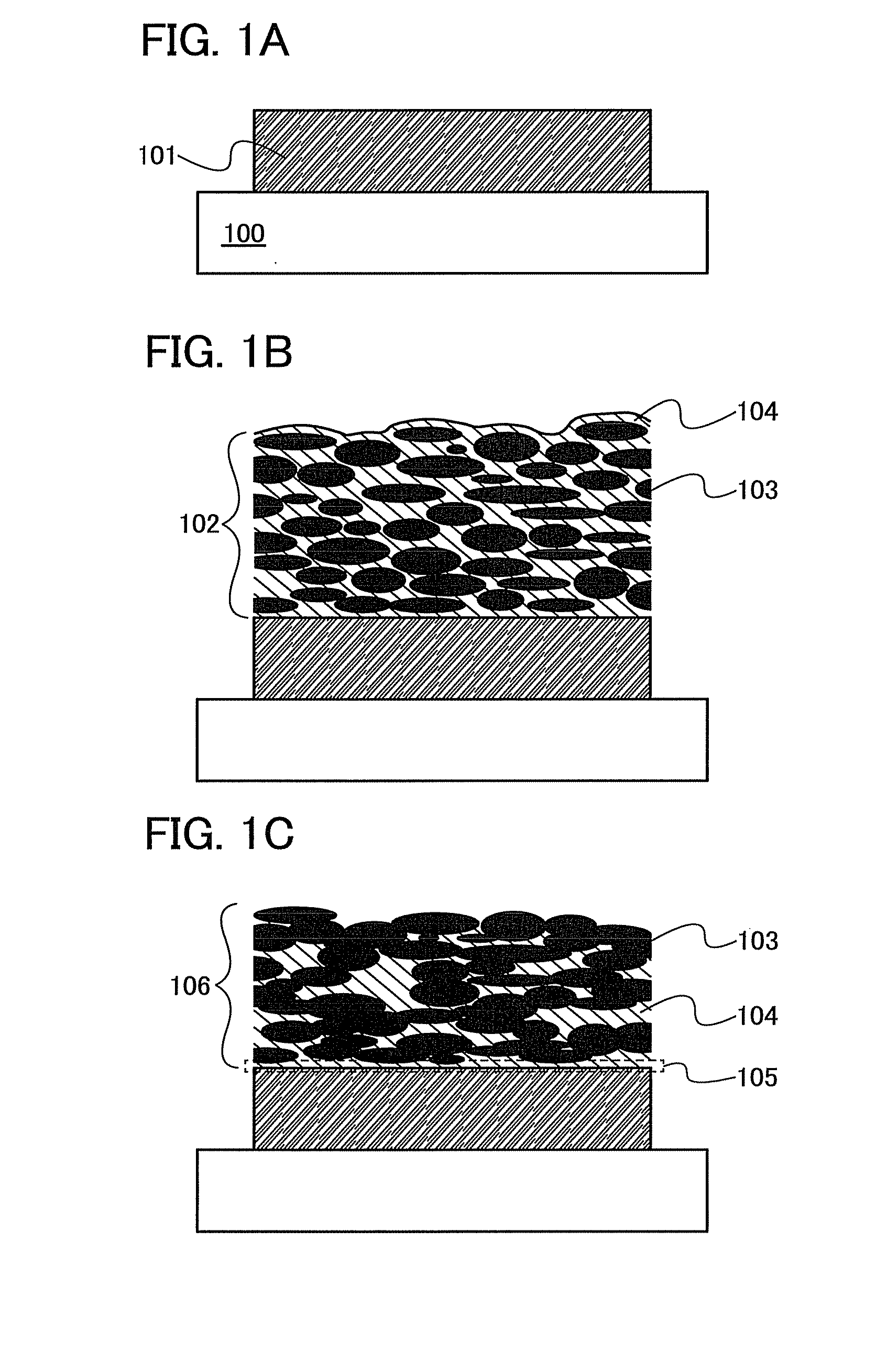
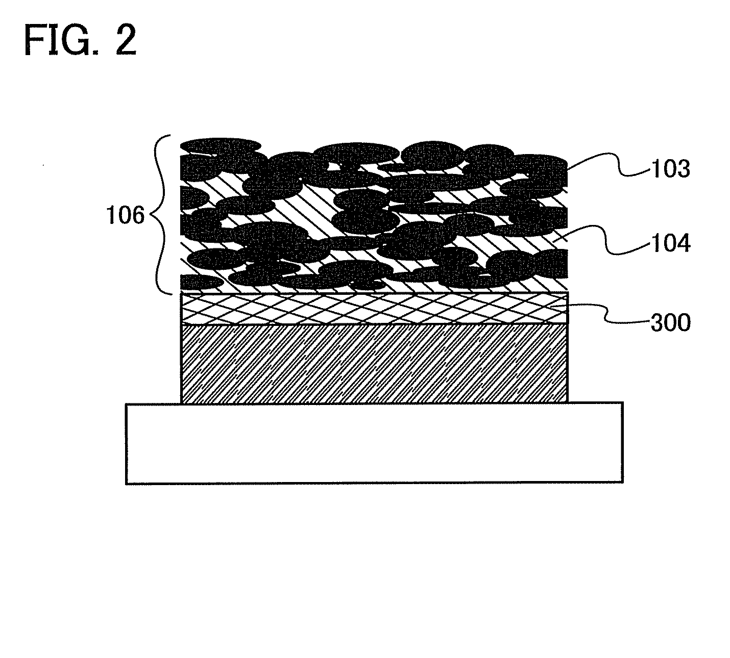
[0048]A memory element and a method for manufacturing the memory element will be described with reference to FIGS. 1A to 1C.
[0049]First, a first conductor 101 is formed over a substrate 100 (see FIG. 1A).
[0050]A substrate formed of any type of material can be used as the substrate 100 as long as the substrate has an insulating property and can hold a manufactured element, like a glass substrate, a plastic substrate, a ceramic substrate, or the like.
[0051]As examples of materials with high conductivity which can be used for the first conductor 101, the following can given: metal such as gold, silver, platinum, nickel, tungsten, palladium, aluminum, manganese, titanium, or tantalum; nitride of the above metal (e.g., titanium nitride, tungsten nitride, or molybdenum nitride); alkali metal such as lithium or cesium belonging to Group of the periodic table, or alkali earth metal such as magnesium, calcium, or strontium belonging to Group 2 of the periodic table; an alloy including any of...
embodiment 2
[0086]In this embodiment, a semiconductor device including the memory element described in Embodiment 1, typically a memory device, will be described with reference to drawings. Note that a passive matrix memory device will be described in this embodiment.
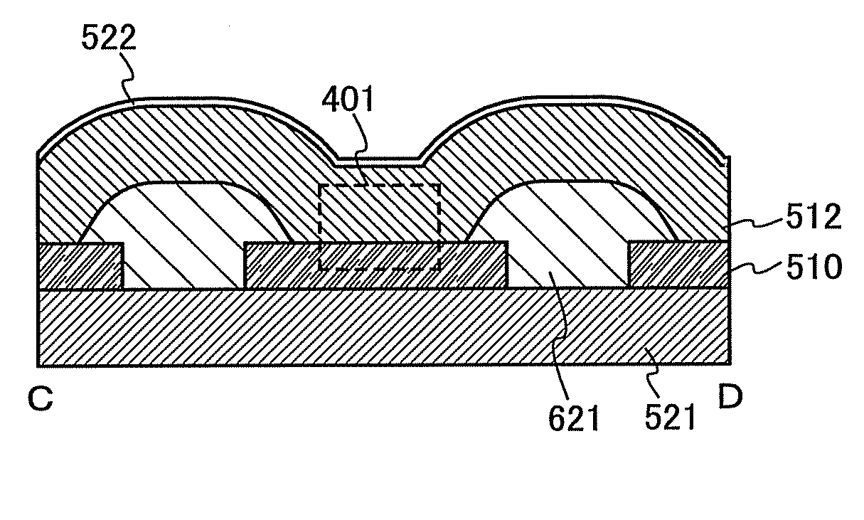
[0087]An example of a structure of a semiconductor device described in this embodiment is illustrated in FIG. 4A. A semiconductor device 400 includes a memory cell array 411 where memory elements 401 are arranged in matrix, decoders 412 and 413, a selector 414, and a read / write circuit 415. The structure of the semiconductor device 400 which is described here is only an example and the semiconductor device 400 may also include other circuits such as a sense amplifier, an output circuit, or a buffer.
[0088]Note that the decoders 412 and 413, the selector 414, the read / write circuit 415, an interface, and the like may also be formed over a substrate as with the memory element. Alternatively, they may be attached externally as IC chips...
embodiment 3
[0117]In this embodiment, a semiconductor device including the memory element of Embodiment 1 will be described with reference to FIGS. 7A to 7C. Specifically, an active matrix memory device will be described in this embodiment.
[0118]An example of a structure of a semiconductor device described in this embodiment is illustrated in FIG. 7A. A semiconductor device 700 includes a memory cell array 711 where memory cells 701 are arranged in matrix, decoders 712 and 713, a selector 714, and a read / write circuit 715. The structure of the semiconductor device 700 which is described here is only one example and the semiconductor device 700 may also include other circuits such as a sense amplifier, an output circuit, or a buffer.
[0119]Note that the decoders 712 and 713, the selector 714, the read / write circuit 715, an interface, and the like may also be formed over a substrate as with the memory element. Alternatively, they may be attached externally as IC chips.
[0120]The memory cell 701 inc...
PUM
 Abstract
Description
Claims
Application Information
 - R&D
- Intellectual Property
- Life Sciences
- Materials
- Tech Scout
- Unparalleled Data Quality
- Higher Quality Content
- 60% Fewer Hallucinations
Browse by: Latest US Patents, China's latest patents, Technical Efficacy Thesaurus, Application Domain, Technology Topic, Popular Technical Reports.
© 2025 PatSnap. All rights reserved.Legal|Privacy policy|Modern Slavery Act Transparency Statement|Sitemap|About US| Contact US: help@patsnap.com