Transparent conductive laminate and touch panel equipped with it

a technology of transparent conductive laminate and touch panel, which is applied in the direction of conductive layers on insulating supports, discharge tubes luminescnet screens, instruments, etc., can solve the problems of lack of reliability in the structure and improve the durability of surface contact pressur

Active Publication Date: 2010-01-07
NITTO DENKO CORP
View PDF14 Cites 19 Cited by
  • Summary
  • Abstract
  • Description
  • Claims
  • Application Information

AI Technical Summary

Benefits of technology

[0020]In the transparent conductive laminate of the invention, a transparent laminated substrate including at least two transparent base films laminated with a transparent pressure-sensitive adhesive layer interposed therebetween is provided on the transparent conductive thin film-free side of the transparent film substrate. This feature can improve not only the pen-input durability but also the surface contact pressure durability, for example, when the transparent conductive laminate is used for touch panels.
[0021]In addition, the dielectric thin film includes a first transparent dielectric thin film of SiOx (wherein x is from 1.5 to less than 2) with a relative refractive index of 1.6 to 1.9 and a second transparent dielectric thin film of SiO2. This feature also improves the surface contact pressure durability. The first transparent dielectric thin film is preferably formed by a dry process.
[0022]In the transparent conductive laminate, the surface contact pressure durability can be further improved by providing the transparent conductive thin film on the film substrate side with the dielectric thin film interposed therebetween. The formation of the dielectric thin film including the first dielectric thin film and second dielectric thin film on the film substrate side is also preferred to further improve the surface contact pressure durability.
[0023]Further, as described above, the SiOx film provided as the first transparent dielectric thin film between the film substrate and the SiO2 film as the second transparent dielectric thin film can reduce the rate of change of the surface electric resistance of the conductive thin film so that a transparent conductive laminate with a high level of stability can be obtained.
[0024]Further, the thickness of the SiOx film may be set in the range of 1 to 30 nm so that the SiOx film can be stably produced in the form of a continuous coating film, while waving or curling can be reduced even under high-temperature and high-humidity conditions, and consequently, changes in reflection characteristics or transmitted hue can be reduced. In addition, the SiOx film formed by a dry process has a high level of moisture resistance or heat resistance, because moisture intrusion into the film substrate can be reduced by the dry process as compared with the case where the SiOx film is formed by a wet process including application of polysiloxane-based thermosetting resin, silica sol, or the like. As a result, waving or curling can be further reduced as compared with conventional cases. Further, the thickness of the SiO2 film may be set in the range of 10 to 70 nm so that the SiO2 film can be stably produced in the form of a continuous coating film, while improvements in abrasion resistance and transparency or a reduction in cracking can be achieved. Further, the thickness of the conductive thin film may also be set in the range of 20 to 35 nm so that the thin film can be stably produced in the form of a continuous coating film, and a reduction in transparency can be suppressed as well as the surface resistance can be reduced.

Problems solved by technology

However, this structure has the problem of lack of reliability, because the surface resistance of the transparent conductive layer is variable.

Method used


Image

  • Transparent conductive laminate and touch panel equipped with it
  • Transparent conductive laminate and touch panel equipped with it
  • Transparent conductive laminate and touch panel equipped with it

Examples


example 1

Formation of Dielectric Thin Films

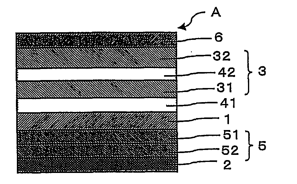
[0087]A SiOx film (1.80 in relative refractive index, 15 nm in thickness) was formed by vacuum deposition on one side of a film substrate made of a 25 μm-thick polyethylene terephthalate film (hereinafter referred to as “PET film”). A SiO2 film (1.46 in relative refractive index, 30 nm in thickness) was then formed on the SiOx film by vacuum deposition.

[0088]Formation of Conductive Thin Film

[0089]A 25 nm-thick ITO film (a conductive thin film, 2.00 in relative refractive index) was then formed on the SiO2 film by reactive sputtering method using a sintered material composed of 95% by weight of indium oxide and 5% by weight of tin oxide in a 0.4 Pa atmosphere composed of 95% of argon gas and 5% of oxygen gas. The ITO film was crystallized by heat treatment at 150° C. for 1 hour.

[0090]Formation of Hard Coat Layer

[0091]A toluene solution as a material for forming a hard coat layer was prepared by adding 5 parts of hydroxycyclohexyl phenyl ketone (Irgac...

example 2

Formation of Dielectric Thin Film

[0097]A 200 nm-thick dielectric thin film of an organic material was formed on one side of a film substrate made of a 25 μm-thick PET film. The dielectric thin film was a cured coating film (with a relative refractive index n of 1.54) of a thermosetting resin composed of a melamine resin, an alkyd resin, and an organosilane condensate (2:2:1 in weight ratio).

[0098]A wet SiO2 film was formed on the dielectric thin film by a silica coating method. Specifically, a silica sol (Colcoat P, manufactured by Colcoat Co., Ltd.) was diluted with ethanol to a solid concentration of 2% and then applied to the dielectric thin film. The coating was dried at 150° C. for 2 minutes and then cured to form a 30 nm-thick wet SiO2 film (with a relative refractive index of 1.46).

[0099]Preparation of Transparent Conductive Laminate

[0100]A transparent conductive laminate was prepared using the process of Example 1, except that the process described above in the section “Form...

example 3

Formation of Dielectric Thin Film

[0101]A dielectric thin film was formed using the process of Example 2, except that the thickness of the dielectric thin film made of the organic material was 35 nm and that the wet SiO2 film was not formed.

[0102]Preparation of Transparent Conductive Laminate

[0103]A transparent conductive laminate was prepared using the process of Example 2, except that the process described above in the section “Formation of Dielectric Thin Film” was performed.


PUM

PropertyMeasurementUnit
relative refractive indexaaaaaaaaaa
thicknessaaaaaaaaaa

Abstract

The transparent conductive laminate of the present invention is a transparent conductive laminate, comprising: a transparent film substrate; a transparent conductive thin film provided on one side of the transparent film substrate with a dielectric thin film interposed therebetween; and a transparent substrate bonded to another side of the transparent film substrate with a transparent pressure-sensitive adhesive layer interposed therebetween, wherein the transparent substrate comprises at least two transparent base films laminated with the transparent pressure-sensitive adhesive layer interposed therebetween, and the dielectric thin film comprises a first transparent dielectric thin film consisting of a SiOx (x is from 1.5 to less than 2) film having a relative refractive index of 1.6 to 1.9, and a second transparent dielectric thin film consisting of a SiO2 film. This feature can improve the surface contact pressure durability.

Description

TECHNICAL FIELD[0001]The present invention relates to a transparent conductive laminate including a film substrate and a conductive thin film provided on the film substrate and having transparency in the visible light range. Also, the present invention relates to a touch panel equipped with the transparent conductive laminate. The transparent conductive laminate of the invention may be used for transparent electrodes in display systems, such as liquid crystal displays and electroluminescence displays, and touch panels, and also used for prevention of static charge of transparent products or electromagnetic wave shielding.BACKGROUND ART[0002]Touch panels can be classified according to the position sensing method into an optical type, an ultrasonic type, a capacitive type, a resistive film type, and the like. In particular, the resistive film type has a simple structure and thus is cost-effective so that it has come into wide use in recent years. For example, resistive film type touch...

Claims


Application Information

Patent Timeline
Patent Type & Authority Applications(United States)
IPC IPC(8): B32B5/16B32B17/06B32B5/00B32B7/023
CPCB32B7/02G06F3/0414B32B5/16B32B7/12B32B2264/102B32B2307/202Y10T428/265B32B2307/536Y10T428/26Y10T428/24942Y10T428/269Y10T428/256B32B2307/412B32B7/023G06F3/045H01B5/14
Inventor NASHIKI, TOMOTAKESUGAWARA, HIDEOYOSHITAKE, HIDETOSHI
Owner NITTO DENKO CORP
Why Eureka
Try Eureka