Group iii nitride semiconductor light-emitting device and epitaxial wafer

a technology of semiconductor light-emitting devices and nitride semiconductors, which is applied in semiconductor devices, semiconductor lasers, laser details, etc., can solve the problems of poor quantum efficiency of light emission and low resistance of hole-blocking layers, and achieve high crystal quality and reduce stress

Inactive Publication Date: 2010-01-14
SUMITOMO ELECTRIC IND LTD
View PDF9 Cites 28 Cited by
  • Summary
  • Abstract
  • Description
  • Claims
  • Application Information

AI Technical Summary

Benefits of technology

[0023]Preferably, in the group III nitride semiconductor light-emitting device of the present invention, the well layers comprise InXGa1−XN, the indium content X of the well layers may be equal to or more than 0.15. The group III nitride semiconductor light-emitting device can emit long-wavelength light. In combination with a hole-blocking layer of a quaternary mixed crystal, the well layers of high crystal quality can be grown even when its indium content is high.
[0024]The group III nitride semiconductor light-emitting device of the present invention may further include a gallium nitride based semicon...

Problems solved by technology

Accordingly, in light emitting diodes prepared on semipolar substrates, holes injected into active layers may overflow from the active layers, resulting in poor quantum efficiency of light emission.
Furthermore, since the thickness of the hol...

Method used


Image

  • Group iii nitride semiconductor light-emitting device and epitaxial wafer
  • Group iii nitride semiconductor light-emitting device and epitaxial wafer
  • Group iii nitride semiconductor light-emitting device and epitaxial wafer

Examples


Embodiment Construction

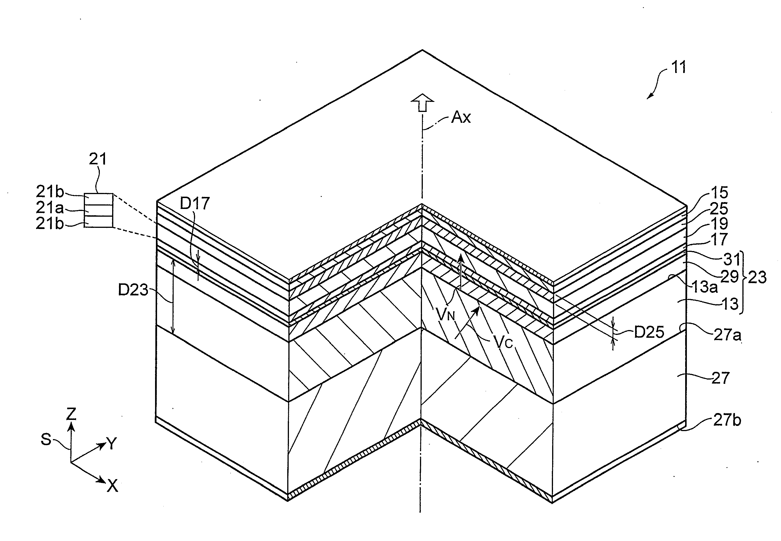
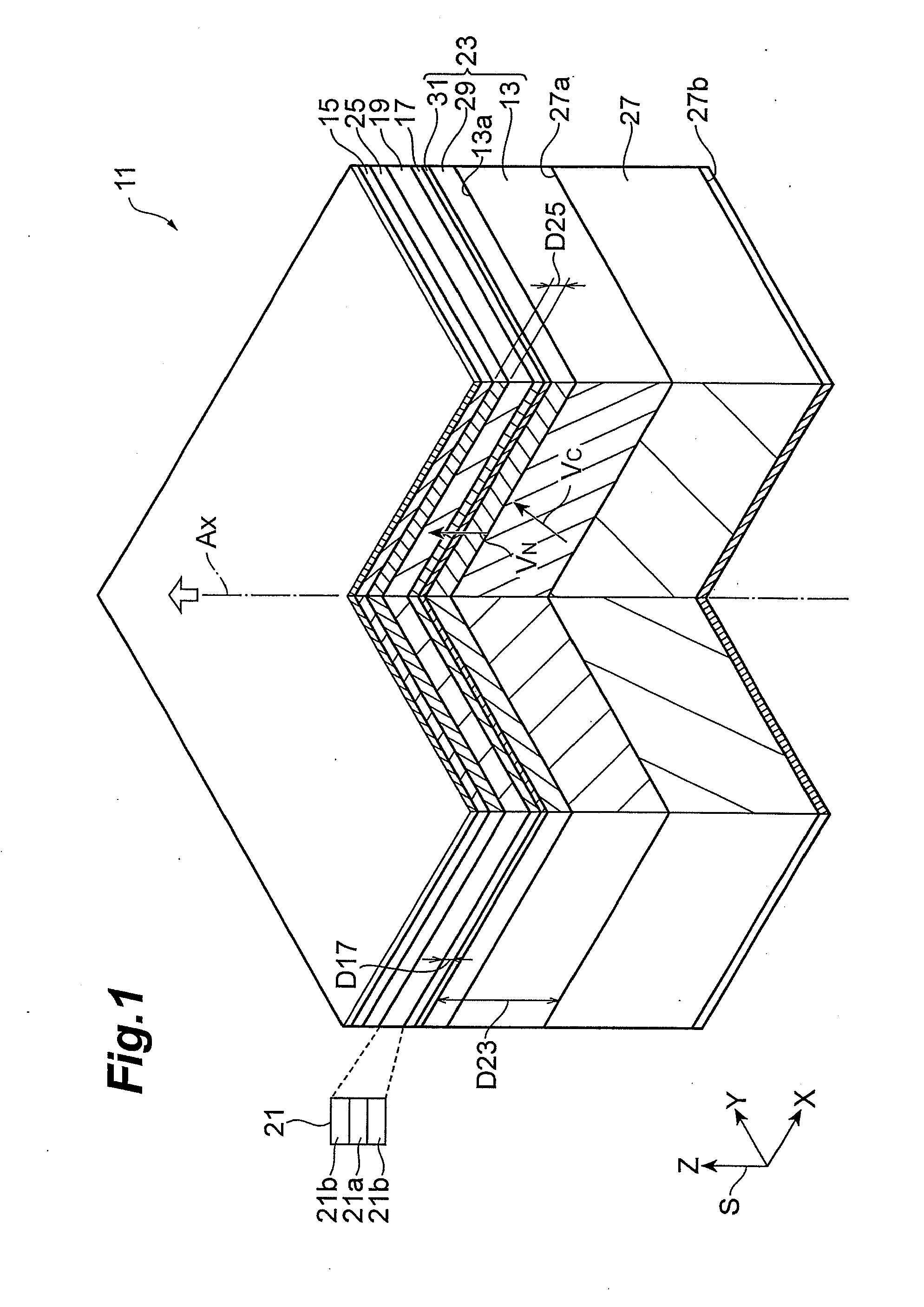
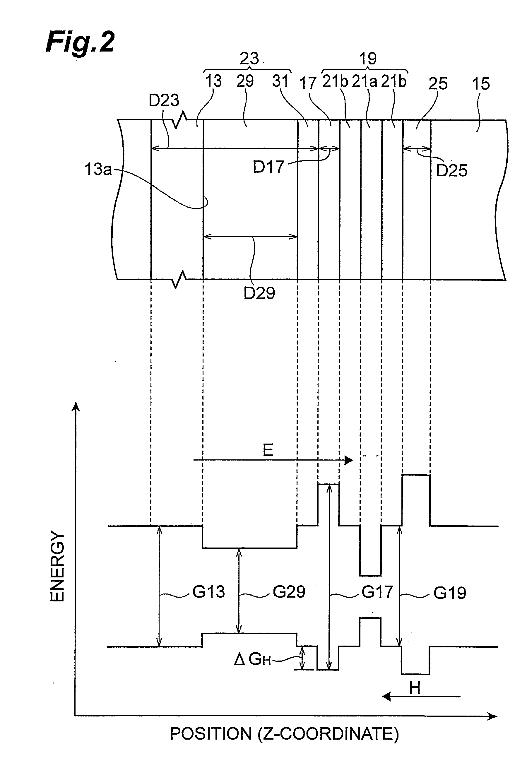
[0037]The teachings of the present invention will readily be understood in view of the following detailed description with reference to the accompanying drawings illustrated by way of example. The embodiments of the group III nitride semiconductor light-emitting device and the epitaxial wafer of the present invention will now be described with reference to the attached drawings. When possible, parts identical to each other will be referred to with reference symbols identical to each other.

[0038]FIG. 1 is a schematic view showing the structure of a group III nitride semiconductor light-emitting device according to an embodiment of the present invention. With reference to FIG. 1, orthogonal coordinate system S for the group III nitride semiconductor light-emitting device 11 (hereinafter referred to as “light-emitting device”) is depicted. FIG. 2 is a view showing a band diagram of the light-emitting device 11. The light-emitting device 11 may be, for example, a light emitting diode. T...


PUM


Abstract

The group II nitride semiconductor light-emitting device includes: a gallium nitride based semiconductor region of n-type; a p-type gallium nitride based semiconductor region; a hole-blocking layer; and an active layer. The gallium nitride based semiconductor region of n-type has a primary surface, and the primary surface extends on a predetermined plane. The c-axis of the gallium nitride based semiconductor region tilts from a normal line of the predetermined plane. The hole-blocking layer comprises a first gallium nitride based semiconductor. The band gap of the hole-blocking layer is greater than the band gap of the gallium nitride based semiconductor region, and the thickness of the hole-blocking layer is less than the thickness of the gallium nitride based semiconductor region. The active layer comprises a gallium nitride semiconductor. The active layer is provided between the p-type gallium nitride based semiconductor region and the hole-blocking layer. The hole-blocking layer and the active layer is provided between the primary surface of the gallium nitride based semiconductor region and the p-type gallium nitride based semiconductor region. The band gap of the hole-blocking layer is greater than a maximum band gap of the active layer.

Description

BACKGROUND OF THE INVENTION [0001]1. Field of the Invention[0002]The present invention relates to a group III nitride semiconductor light-emitting device and an epitaxial wafer.[0003]2. Description of the Related Art[0004]Patent publication 1 (Japanese Unexamined Patent Application Publication No. 6-260683) discloses a blue light emitting diode of a double heterostructure. A low-temperature buffer layer composed of GaN is provided on a substrate composed of a different material, for example, sapphire, SiC, or ZnO. An n-type GaN layer (first cladding layer), a Zn-doped InGaN layer (emitting layer), and a Mg-doped p-type GaN layer (second cladding layer) are grown in sequence on the buffer layer.SUMMARY OF THE INVENTION [0005]The blue light emitting device disclosed in Patent publication 1 includes the InGaN emitting layer grown on a c-plane sapphire substrate. A group III nitride semiconductor light-emitting device such as a blue light emitting diode can be formed on a c-plane GaN su...

Claims


Application Information

Patent Timeline
IPC IPC(8): H01S5/323
CPCH01L33/32H01L33/06
Inventor ENYA, YOHEIKYONO, TAKASHIAKITA, KATSUSHIUENO, MASAKI
Owner SUMITOMO ELECTRIC IND LTD
Why Eureka
Try Eureka