
Hybrid Strip-Loaded Electro-Optic Polymer/Sol-Gel Modulator

a polymer and hybrid technology, applied in the field of hybrid eo polymer/solgel modulator, to achieve the effect of improving extinction and reducing insertion loss

Inactive Publication Date: 2010-01-21
THE ARIZONA BOARD OF REGENTS ON BEHALF OF THE UNIV OF ARIZONA
View PDF7 Cites 5 Cited by
  • Summary
  • Abstract
  • Description
  • Claims
  • Application Information

AI Technical Summary

Benefits of technology

[0018]The present invention provides hybrid EO polymer / sol-gel modulators with higher electric field / optical field overlap factor Γ and smaller inter-electrode separation d to reduce the modulator's half-wave drive voltage Vπ, reduce insertion loss and improve extinction. This is accomplished with modulator designs in which the sol-gel core waveguide does not lie below the EO polymer waveguide in the active region.
[0020]In a first index-tapered, core-tapered embodiment, the sol-gel over cladding has been eliminated and the vertical taper formed in the sol-gel core. Placing the EO polymer waveguide in the same plane as the sol-gel core eliminates the potential for deleterious coupling between the sol-gel core and the EO polymer waveguide. The EO polymer waveguide is physically extended to cover the vertical taper in the passive regions on either side of the active region. The index itself is tapered from a high uniform value in the active region to a lower value to approximately match the sol-gel core at the top of the taper. By tapering the EO polymer waveguide index the inter-electrode separation d is reduced and the electric field / optical field overlap factor Γ is increased, both having the beneficial effect of reducing the half-wave drive voltage. The formation of the vertical taper in the sol-gel core and the index taper of the EO polymer waveguide are separable features.
[0021]In a second phantom-core embodiment, the sol-gel core lies in a plane below the plane of the EO polymer waveguide. The sol-gel core is patterned so that the core waveguide stops at or near the end of the vertical taper in the sol-gel over cladding. The gap that is created is filled with a sol-gel or other material with a refractive index less than or equal to that of the sol-gel under cladding. Since this region is no longer a waveguide, no light is coupled from the EO polymer waveguide to the core thereby increasing Γ and reducing coupling to the bottom electrode. In fact, the bottom electrode may be placed on top of the sol-gel under cladding for reduced inter-electrode separation d. The lack of background light from the sol-gel core leads to significantly improved modulation efficiency as well.
[0022]In a third transverse-tapered embodiment, a sol-gel side-cladding lies in the same plane as the sol-gel core. The side-cladding has a transverse physical taper on one (phase modulator) or both (Mach-Zehnder modulator) sides of the sol-gel core that defines a gap on one or both sides of the core. The gap increases gradually from the core from both ends until reaching a fixed gap that is maintained over the active region of the modulator. The gap(s) between the sol-gel core and sol-gel side-cladding are filled with EO polymer to form an EO polymer waveguide. A buffer layer lies over the EO polymer. A top electrode and patterned bottom electrode define the active region there between. This transverse-taper design improves confinement in the EO polymer waveguide so that the inter-electrode spacing can be reduced and Γ increased. The transverse physical taper can be formed using standard lithographic techniques. The performance can be improved by tapering the refractive index of the EO polymer waveguide to gradually increase from a value slightly above that of the sol-gel core to its ordinary high value in the active region of the EO modulator.
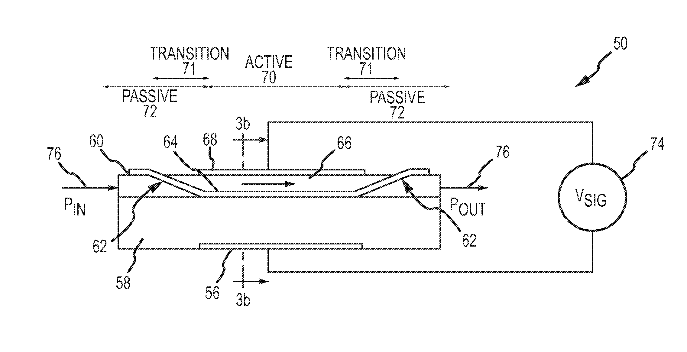
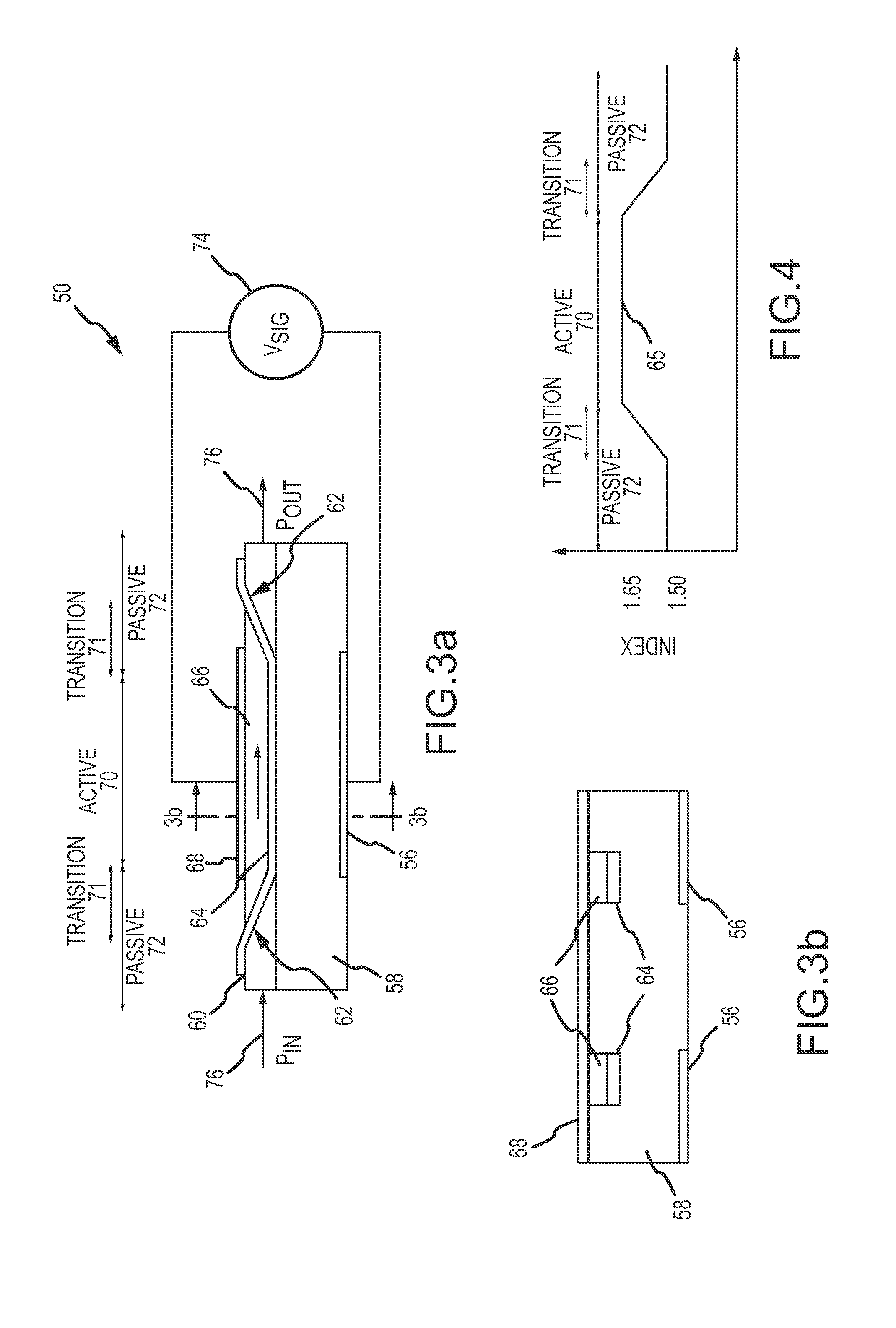
[0023]A fourth strip-loaded embodiment comprises a sol-gel under cladding having a refractive index n1, a sol-gel core having a refractive index n2>n1 and a sol-gel side cladding having a refractive index n3≈n1<n2 in the same plane as the sol-gel core. An EO polymer layer is provided with a graded refractive index. The EO polymer has an index n4<n2 in a first passive region that provides a top cladding for the sol-gel core to define a first sol-gel waveguide in the first passive region. The index is graded in a first transition region from n4 up to n5>n2 in an active region so that the sol-gel core provides a bottom cladding for the EO polymer layer to define an EO polymer waveguide in the active region, The index is graded in a second transition region from n5 down to n6<n2 in a second passive region that provides a top cladding for the sol-gel core to define a second sol-gel waveguide in the second passive region. A sol-gel buffer layer lies above the EO polymer layer and has a refractive index n7<n5 in the active region. First and second electrodes on opposite sides of the EO polymer waveguide in the active region are configured to receive a voltage signal to apply an electric field along the poling direction to change the refractive index of the EO polymer waveguide in the active region. The use of a uniform thickness EO polymer layer eliminates optical scattering caused by sidewall roughness due to etching, thereby leading to lower optical propagation loss in the active section. The sol-gel core also acts as a virtual side-cladding to confine light laterally in the overlying EO polymer layer thereby creating a well defined EO polymer waveguide in the active region for efficient coupling back into the sol-gel waveguide for coupling to optical fiber.

Problems solved by technology

EO modulators are generally used when direct modulation of the laser in the communications system is not a viable option, which occurs when very high bandwidth (>10 GHz) or signal linearity are required.

Method used


Image

  • Hybrid Strip-Loaded Electro-Optic Polymer/Sol-Gel Modulator
  • Hybrid Strip-Loaded Electro-Optic Polymer/Sol-Gel Modulator
  • Hybrid Strip-Loaded Electro-Optic Polymer/Sol-Gel Modulator

Examples


Embodiment Construction

[0040]The present invention describes hybrid EO polymer / sol-gel modulators with higher electric field / optical field overlap factor Γ and smaller inter-electrode separation d to reduce the modulator's half-wave voltage Vπ, reduce insertion loss and improve extinction. Applications for these new designs include but are not limited to high speed analog modulators for cable TV, phased array radars, photonic analog-to-digital converts, RF photonics, fiber optic gyroscopes and true time delay lines as well as digital modulators for optical communications networks ranging from long haul dense wavelength division multiplexing (DWDM) networks, to metropolitan area DWDM, to passive optical networks (PON) for optical access.

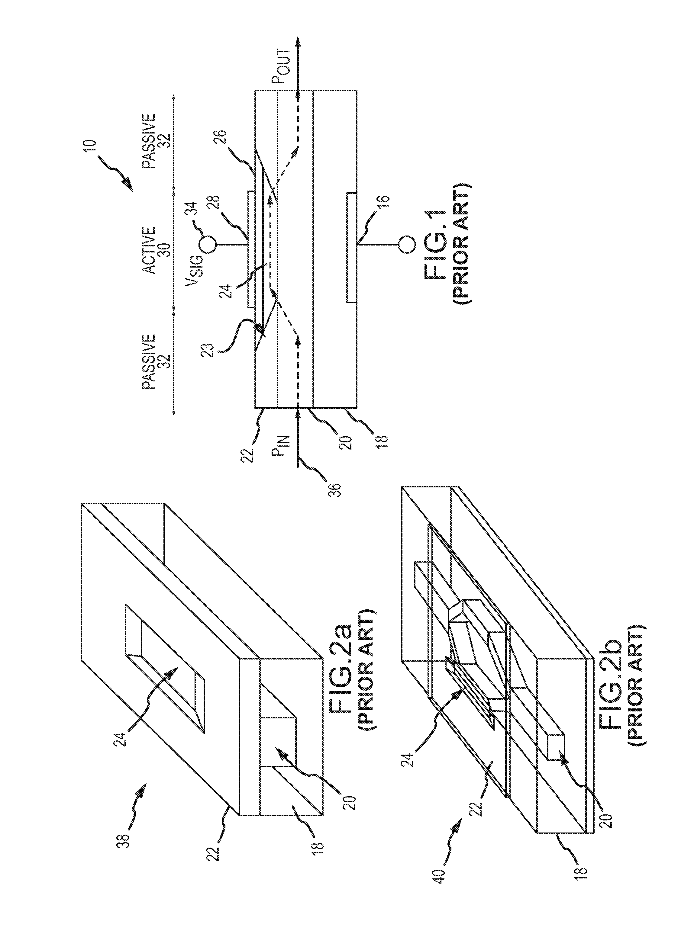
[0041]The conventional design of the hybrid EO polymer / sol-gel modulator as illustrated in FIG. 1 suffers from several limitations owing principally to the fact that the design employs a sol-gel core waveguide that lies directly below the active EO polymer waveguide—this ha...


PUM


Abstract

A hybrid strip-loaded EO polymer / sol-gel modulator in which the sol-gel core waveguide does not lie below the active EO polymer waveguide increases the higher electric field / optical field overlap factor Γ and reduces inter-electrode separation d thereby lowering the modulator's half-wave drive voltage Vπ, reducing insertion loss and improving extinction. The strip-loaded modulator comprises an EO polymer layer that eliminates optical scattering caused by sidewall roughness due to etching. Light does not encounter rough edges as it transitions to and from the sol-gel and EO polymer waveguides. This reduces insertion loss.

Description

CROSS-REFERENCE TO RELATED APPLICATIONS[0001]This application claims benefit of priority under 35 U.S.C. 120 as a continuation-in-part of co-pending U.S. application Ser. No. 12 / 199,765 entitled “Hybrid Electro-Optic Polymer / Sol-Gel Modulator” filed Aug. 27, 2008, which claims benefit of priority under 35 U.S.C. 119(e) to U.S. Provisional Application No. 60 / 967,679 entitled “Hybrid Electro-Optic Polymer / Sol-Gel Modulators With Reduced Half-Wave Voltage, Lower Insertion Loss and Improved Contrast” and filed on Sep. 6, 2007, the entire contents of which are incorporated by reference.GOVERNMENT LICENSE RIGHTS[0002]This invention was made with government support under NR0000-07-C-0030 awarded by the Department of Defense and under DMR0120967 awarded by the National Science Foundation. The government has certain rights in the invention.BACKGROUND OF THE INVENTION[0003]1. Field of the Invention[0004]This invention relates to electro-optic (EO) modulators and more particularly to hybrid EO...

Claims


Application Information

Patent Timeline
IPC IPC(8): G02F1/035
CPCG02F1/065G02F1/225G02F2202/07G02F2201/07G02F2201/066
Inventor DEROSE, CHRISTOPHER T.HIMMELHUBER, ROLANDNORWOOD, ROBERT A.PEYGHAMBARIAN, NASSER N.
Owner THE ARIZONA BOARD OF REGENTS ON BEHALF OF THE UNIV OF ARIZONA
Learn More