Plasma processing apparatus and plasma processing method

a processing apparatus and plasma technology, applied in the direction of fluid pressure measurement, fluid pressure measurement by optical means, instruments, etc., can solve the problems of affecting the quality of plasma, the shape of the wafer edge is not uniform, and the adjacent capacitors come into contact, etc., to achieve stable suppression of the tilt of the hole, reduce the height difference, and reduce the number of inferior products

Inactive Publication Date: 2010-02-04
HITACHI HIGH-TECH CORP
View PDF0 Cites 59 Cited by
  • Summary
  • Abstract
  • Description
  • Claims
  • Application Information

AI Technical Summary

Benefits of technology

[0015]A plasma processing apparatus and a plasma processing method according to the present invention involve simply monitoring the amount of consumption of a focus ring disposed along the perimeter of a wafer. Thus, for example, in a case where high-aspect-ratio contact holes are to be formed as a pattern, the amount of the RF bias electric power separately applied to the focus ring to reduce the height difference between the ion s...

Problems solved by technology

However, it is difficult to ensure that the bottom part of the pattern of a miniaturized capacitor has adequate mechanical strength by itself, and there is a problem that adjacent capacitors come into contact with each other.
In this process, an abnormality in shape of the wafer edge poses a problem. FIG. 5 shows states of an edge region of a wafer.
However, according to these inv...

Method used


Image

  • Plasma processing apparatus and plasma processing method
  • Plasma processing apparatus and plasma processing method
  • Plasma processing apparatus and plasma processing method

Examples


first embodiment

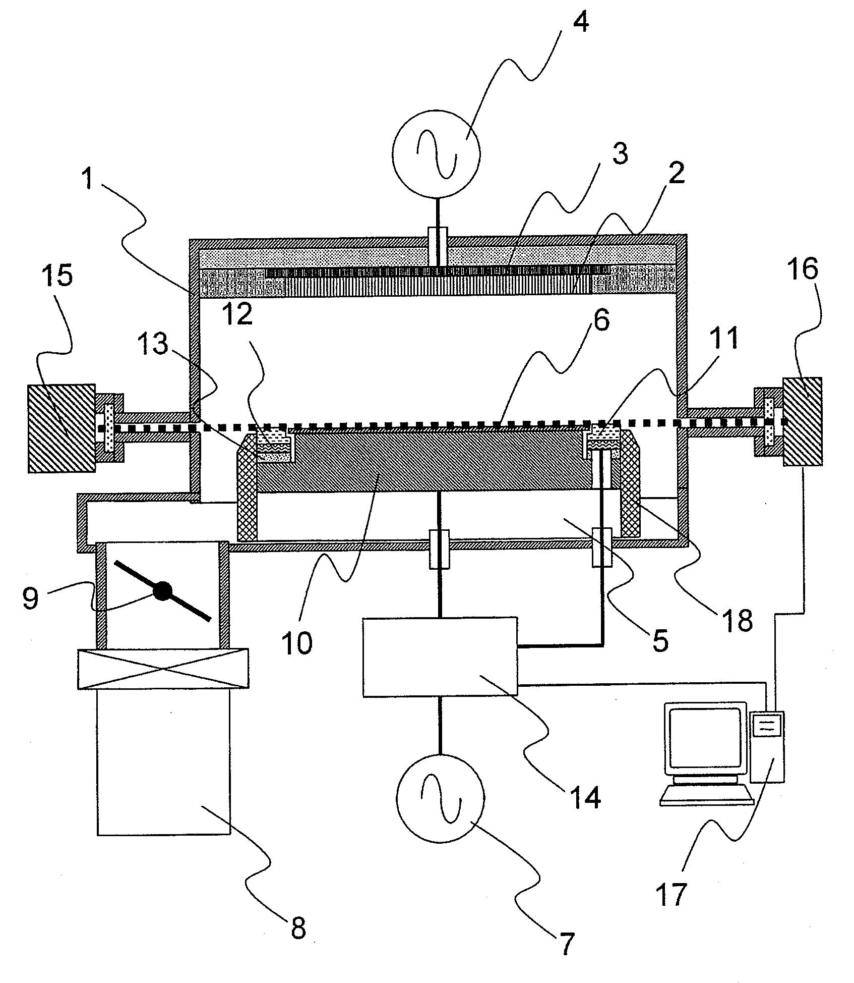
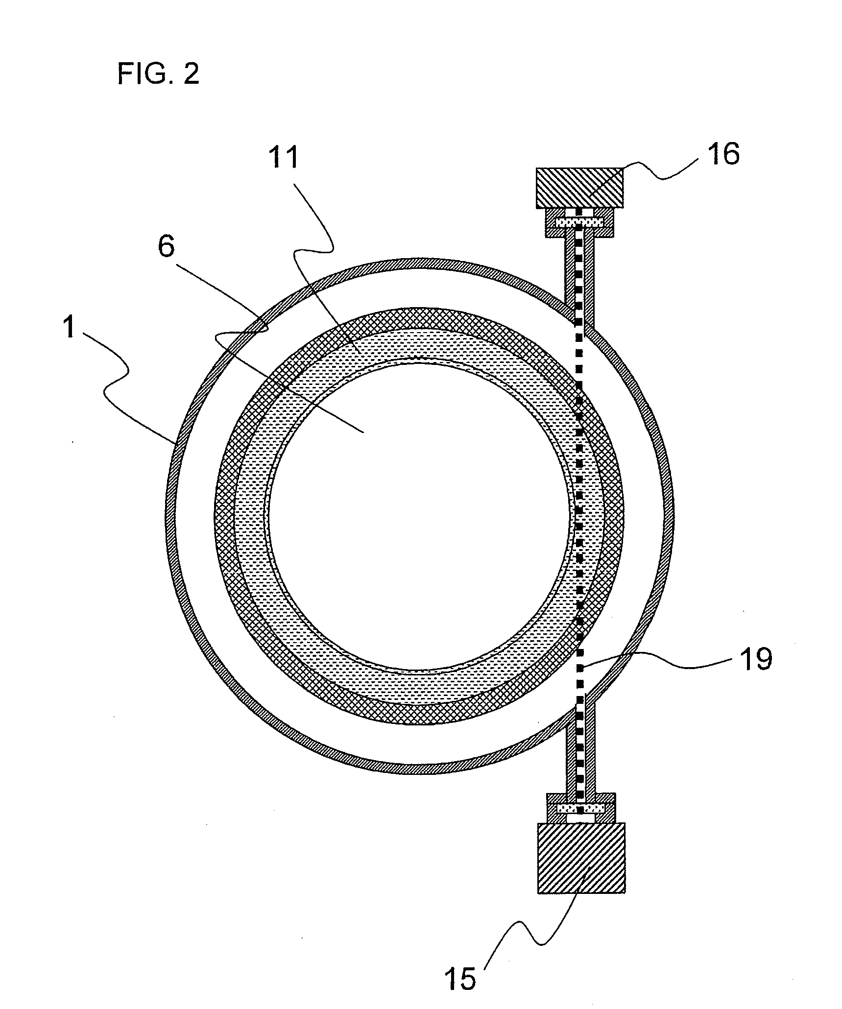
[0033]In the following, a first embodiment of the present invention will be described with reference to the drawings. In the first embodiment, there will be described a method of monitoring the amount of consumption of a focus ring using a laser as a light source. FIGS. 1 and 2 are schematic diagrams for illustrating a configuration of a plasma processing apparatus (an etching apparatus) used in the first embodiment. FIG. 1 is a vertical cross-sectional view of the plasma processing apparatus, and FIG. 2 is a horizontal cross-sectional view of the plasma processing apparatus taken along the plane of a wafer. The plasma processing apparatus has a vacuum chamber 1 and a shower plate 2, an upper electrode 3 and a lower electrode 5 housed in the vacuum chamber 1. Furthermore, the vacuum chamber 1 has an evacuation system 8 connected to the vacuum chamber 1 via a conductance valve 9, a light source 15, and light receiving means 16. An annular member 11 (referred to as focus ring hereinaf...

second embodiment

[0048]In the first embodiment, there has been described a method of detecting the amount of consumption of the focus ring using a laser beam having an optical axis parallel with the focus ring surface and the wafer surface. In a second embodiment, there will be described a method of detecting the amount of consumption of the focus ring by obliquely emitting a laser beam to the surface of the focus ring 11 and monitoring the reflected light from the surface of the focus ring 11. FIG. 10 is a schematic vertical cross-sectional view showing a configuration of a plasma processing apparatus used in this embodiment. The horizontal cross section of the plasma processing apparatus taken along the plane of the wafer is substantially the same as that shown in FIG. 2, and the horizontal cross section will be described with reference to FIG. 2. The light source 15 is installed on a side wall of the chamber to emit a laser beam onto the focus ring 11, and the light receiving means 16 is installe...


PUM

PropertyMeasurementUnit
Thicknessaaaaaaaaaa
Wavelengthaaaaaaaaaa
Lightaaaaaaaaaa

Abstract

To monitor the thickness of a focus ring consumed during wafer processing. A plasma processing apparatus includes a vacuum chamber 1, workpiece mounting means 5, high frequency electric power introducing means 4 and radio-frequency bias electric power introducing means 7 and processes a surface of a workpiece 6 using a plasma that is converted from a gas introduced into the vacuum chamber 1 by the action of a high frequency electric power introduced by the high frequency electric power introducing means 4. The plasma processing apparatus further includes an annular member 11 surrounding the workpiece 6 mounted on the workpiece mounting means 5, and a pair of tubes having an aspect ratio of 3 or higher and disposed on a side wall of the vacuum chamber 1 to face each other. Each tube is vacuum-sealed at a tip end thereof with a glass material. One of the tubes has a light source 15 disposed facing to the interior of the vacuum chamber on the atmosphere side of the glass material, and the other tube has light receiving means 16 disposed facing to the interior of the vacuum chamber on the atmosphere side of the glass material. The light receiving means 16 receives light passing across the surface of the annular member 11.

Description

[0001]The present application is based on and claims priority of Japanese patent application No. 2008-196726 filed on Jul. 30, 2008, the entire contents of which are hereby incorporated by reference.BACKGROUND OF THE INVENTION[0002]1. Field of the Invention[0003]The present invention relates to a dry etching apparatus (a plasma processing apparatus) and an etching method (a plasma processing method) used for etching of an interlayer insulating film in an etching process using a plasma processing apparatus. For example, it relates to a plasma processing apparatus and a plasma processing method that can prevent a tilt of a hole, which occurs especially at an edge of a workpiece in a case where the pattern to be formed in the workpiece is a high-aspect-ratio contact hole.[0004]2. Description of the Related Art[0005]For memory devices, such as the dynamic random access memory (DRAM), it is important to maintain the capacitor capacitance when the packaging density increases. In general, ...

Claims


Application Information

Patent Timeline
IPC IPC(8): G01L11/02
CPCH01J37/32642H01J37/3299H01J37/32935
Inventor NEGISHI, NOBUYUKIIZAWA, MASARUMAEDA, KENJI
Owner HITACHI HIGH-TECH CORP
Why Eureka
Try Eureka